Optical device assembly system and method for fixing optical elements

A technology for optical components and assembly systems, applied in the direction of optical components, optics, installation, etc., can solve problems affecting the adjustment of optical components, damage to optical components, and limit the use range, etc., to ensure adjustment accuracy, small defect rate after welding, and avoid Effects of heat damage

Inactive Publication Date: 2009-09-30
PHOEBUS VISION OPTO ELECTRONICS TECH +1
View PDF1 Cites 1 Cited by
  • Summary
  • Abstract
  • Description
  • Claims
  • Application Information

AI Technical Summary

Problems solved by technology

[0003] However, this method of fixing optical components uses a light beam to heat the flux. If the light beam continues to heat the solder during the entire adjustment of the position of the optical component after the flux is melted, the temperature of the solder will be too high, and the optical component may even be damaged; Beam, flux temperature will decrease rapidly, lack of fluidity, directly affect the adjustment of the position of optical components; in addition, because its substrate must be a special transparent material, such as glass, etc., which limits its scope of use

Method used


Image

  • Optical device assembly system and method for fixing optical elements
  • Optical device assembly system and method for fixing optical elements
  • Optical device assembly system and method for fixing optical elements

Examples


Embodiment Construction

[0035] The present invention will be further explained and illustrated below in conjunction with the accompanying drawings.

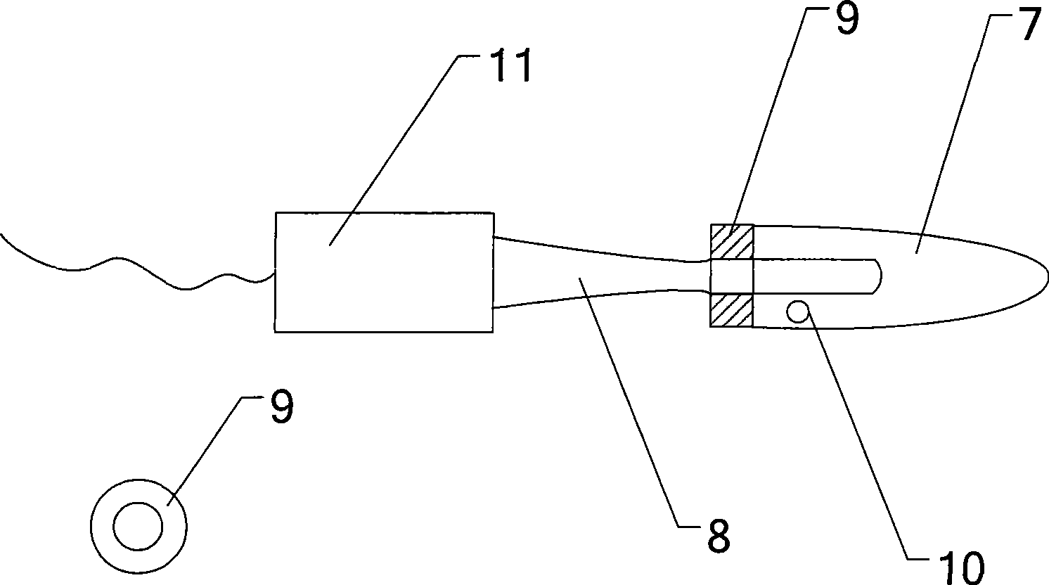
[0036] As an embodiment of the present invention, an optical device assembly system includes an optical element fixing device and an adjustment device for adjusting the position of each optical element, the optical element fixing device includes a control module and is electrically connected to the control module The solder filling device and two temperature control rods are used to melt the solder, and the temperature of the temperature control rods is controlled and adjusted by the control module in the adjustment device.

[0037] As an example, figure 1 A section structure of a temperature control rod is given, including a metal cover 7 , a ceramic heating rod 8 , a semiconductor cooling chip (TEC) 9 , a temperature sensor 10 and a handle 11 . The metal cover 7 is set on the front end of the ceramic heating rod 8, and a temperature sensor 10 electri...


PUM


Abstract

The invention discloses an optical device assembly system and a method for fixing optical elements. An optical device comprises the optical elements and a heat sink; a metal layer is plated on at least one surface of each optical element; the assembly system comprises an optical element fixing device, andoptical element fixing device comprises a control module as well as a solder filling device and at least one temperature control bar which are respectively electrically connected with the control module, wherein the solder filling device is used for filling solder between the metal layers of the optical elements and the heat sink, the temperature control bar is used for melting the solder, and the temperature of the temperature control bar can be controlled by the control module. When being used for melting the solder, the temperature control bar can precisely control the temperature of the solder and avoid the insufficient flowability brought by over low solder temperature, thereby ensuring the adjustment precision; in addition, the heat injury possibly brought by the optical elements can be avoided; the real-time temperature adjustment can be realized by adopting an electric control system, and the temperature of the solder can be adjusted according to the element adjusting state which can be controlled to be in a melted or semi-melted state.

Description

technical field [0001] The invention relates to the field of optical devices, in particular to an optical device assembly system and a method for fixing optical components. Background technique [0002] In the current manufacture of optical instruments and equipment, various optical devices including lenses are directly bonded to the heat sink or base by adhesives. Since the bonding gap is small and there may be a certain inclination, traditional The bonding fluidity of the special adhesive is not enough, and it can only be bonded from the outer periphery to the inside, which will cause a cavity in the middle, not completely bonded, thus lacking stability and fixity, and easy to crack under harsh natural conditions. In order to overcome this difficulty, Chinese patent application publication number CN1591059A discloses an optical device assembly device and a method for fixing optical components thereof, including a base and an optical component fixed on the base. The surfac...

Claims


Application Information

Patent Timeline
Patent Type & Authority Applications(China)
IPC IPC(8): G02B7/00
Inventor 王斌张瑛亓岩毕勇田振清贾中达
Owner PHOEBUS VISION OPTO ELECTRONICS TECH
Why Eureka
Try Eureka