
TFT-LCD array substrate and color film substrate and manufacturing method thereof

An array substrate and color filter substrate technology, applied in the TFT-LCD array substrate and color filter substrate and their manufacturing fields, can solve the problem of affecting the TFT-LCD yield rate, poor TFT-LCD bright lines, and difficult to return to the original position and other problems to achieve the effect of improving display quality, increasing the number of potential connections, and increasing resilience

Active Publication Date: 2009-09-30
BOE TECH GRP CO LTD +1
View PDF0 Cites 31 Cited by
  • Summary
  • Abstract
  • Description
  • Claims
  • Application Information

AI Technical Summary

Problems solved by technology

[0005] (1) The transparent electrode on the color filter substrate and the common electrode on the array substrate can only be connected in an indirect way, that is, it must pass through the peripheral circuit structure outside the pixel area, such as using conductive silver glue or conductive metal balls, etc., and this This connection structure is easy to cause electrostatic breakdown during production, which will cause TFT-LCD to have defects such as poor bright lines;
[0006] (2) Since the contact position between the columnar spacer and the array substrate is at the highest position of the array substrate (above the TFT), when the substrate is squeezed or impacted, The columnar spacer will automatically move to a lower position, and it is difficult to return to the original position, resulting in poor light leakage, which seriously affects the yield rate of TFT-LCD, and also has a negative impact on the display effect

Method used


Image

  • TFT-LCD array substrate and color film substrate and manufacturing method thereof
  • TFT-LCD array substrate and color film substrate and manufacturing method thereof
  • TFT-LCD array substrate and color film substrate and manufacturing method thereof

Examples


Embodiment Construction

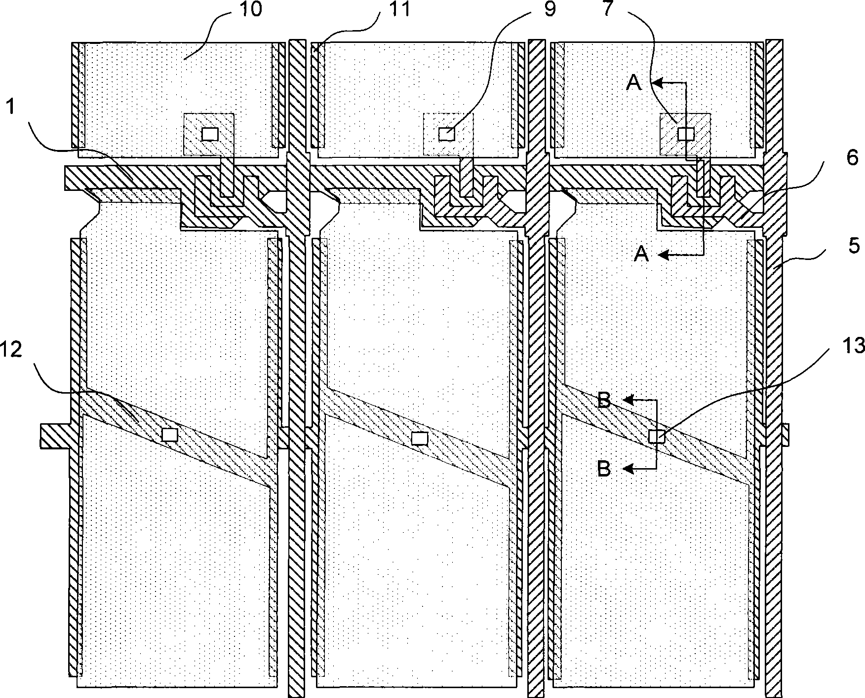
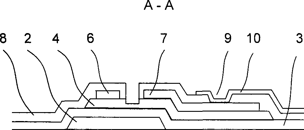
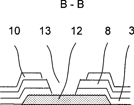
[0040] Figure 1a It is a structural schematic diagram of the TFT-LCD array substrate of the present invention, Figure 1b for Figure 1a Middle A-A section view, Figure 1c for Figure 1a Middle B-B section view. Such as Figure 1a , Figure 1b and Figure 1c As shown, gate lines 1, data lines 5 and common electrode lines 12 are formed on the TFT-LCD array substrate of the present invention, the common electrode lines 12 are arranged between two gate lines 1, and the data lines 5 are perpendicular to the gate lines 1 and adjacent to each other. The gate line 1 and the data line 5 define a pixel area, and form a TFT at the intersection, and the TFT is composed of a gate electrode 2, a gate insulating layer 3, an active layer 4, a source electrode 6 and a drain electrode 7, wherein the gate electrode 2 It is connected to the gate line 1, the source electrode 6 is connected to the data line 5, the pixel electrode 10 located in the pixel area is connected to the drain electrod...


PUM

PropertyMeasurementUnit
widthaaaaaaaaaa
widthaaaaaaaaaa
heightaaaaaaaaaa

Abstract

The invention relates to a TFT-LCD array substrate and a color film substrate. The array substrate comprises a grid line, a common electrode line and a data line which are formed on the array substrate, a TFT formed at the intersection between the grid line and the data line, and a pixel electrode positioned in the pixel area, wherein a second passivation layer through hole and a pixel electrode through hole which enable the common electrode line to be exposed out are arranged on the common electrode line and are used for being electrically connected with a transparent electrode on the color film substrate. The color film substrate comprises a black matrix, color resin, a cylindrical spacer and a transparent electrode which are formed on the color film substrate, wherein the cylindrical spacer is arranged at the position corresponding to the second passivation layer through hole on the array substrate, and the transparent electrode is covered on the cylindrical spacer. The invention changes the electric connection way of the transparent electrode on the color film substrate and the common electrode on the array substrate and improves the display quality of the TFT-LCD.

Description

technical field [0001] The invention relates to a liquid crystal display device and a manufacturing method thereof, in particular to a TFT-LCD array substrate and a color filter substrate and a manufacturing method thereof. Background technique [0002] Thin Film Transistor Liquid Crystal Display (TFT-LCD for short) has the characteristics of small size, low power consumption, no radiation, and relatively low manufacturing cost, and occupies a dominant position in the current flat panel display device market. TFT-LCD is formed by combining an array substrate and a color filter substrate (color filter) into a cell and injecting liquid crystals into it. Columnar spacers are usually set between the array substrate and the color filter substrate to maintain the thickness of the cell. [0003] The prior art array substrate includes gate lines, data lines and common electrode lines formed on the substrate. The data lines are perpendicular to the gate lines. Adjacent gate lines and...

Claims


Application Information

Patent Timeline
Patent Type & Authority Applications(China)
IPC IPC(8): G02F1/1362H01L27/12H01L21/84G02F1/1339
Inventor 张弥
Owner BOE TECH GRP CO LTD
Learn More