Liquid crystal panel

A liquid crystal panel and glass plate technology, applied in nonlinear optics, instruments, optics, etc., can solve the problem of low yield rate of laser cutting process, achieve the effect of balancing internal stress and avoiding deflection cracks

Inactive Publication Date: 2009-09-30
STATE GRID CORP OF CHINA +2
View PDF0 Cites 0 Cited by
  • Summary
  • Abstract
  • Description
  • Claims
  • Application Information

AI Technical Summary

Problems solved by technology

However, in the process of pre-cutting the liquid crystal panel 10 in the x-axis direction, since there are structural differences between the adjacent sides of the cutting line in the x-axis direction on the liquid crystal panel 10, that is, the central area of ​​the thin film transistor unit 110 on one side of the cutting line is 1102 is provided with a frame glue 13 that is bonded to the color filter substrate 12, while the circuit area 1104 of the thin film transistor unit 110 on the other side is not provided with a frame glue 13 that is bonded to the color filter substrate 12. The difference in structure will lead to different stresses inside the liquid crystal panel 10, so there will be obvious cracks 16 in the area between the thin film transistor units 110 cut by the laser along the dotted line 14, and the cracks 16 will usually extend to the area where the sealant 13 is not provided. The line area 1104 of the thin film transistor unit 110, resulting in a low yield rate of the liquid crystal panel laser cutting process

Method used


Image

  • Liquid crystal panel
  • Liquid crystal panel
  • Liquid crystal panel

Examples


Embodiment Construction

[0013] The present invention will be further described in detail below in conjunction with the accompanying drawings.

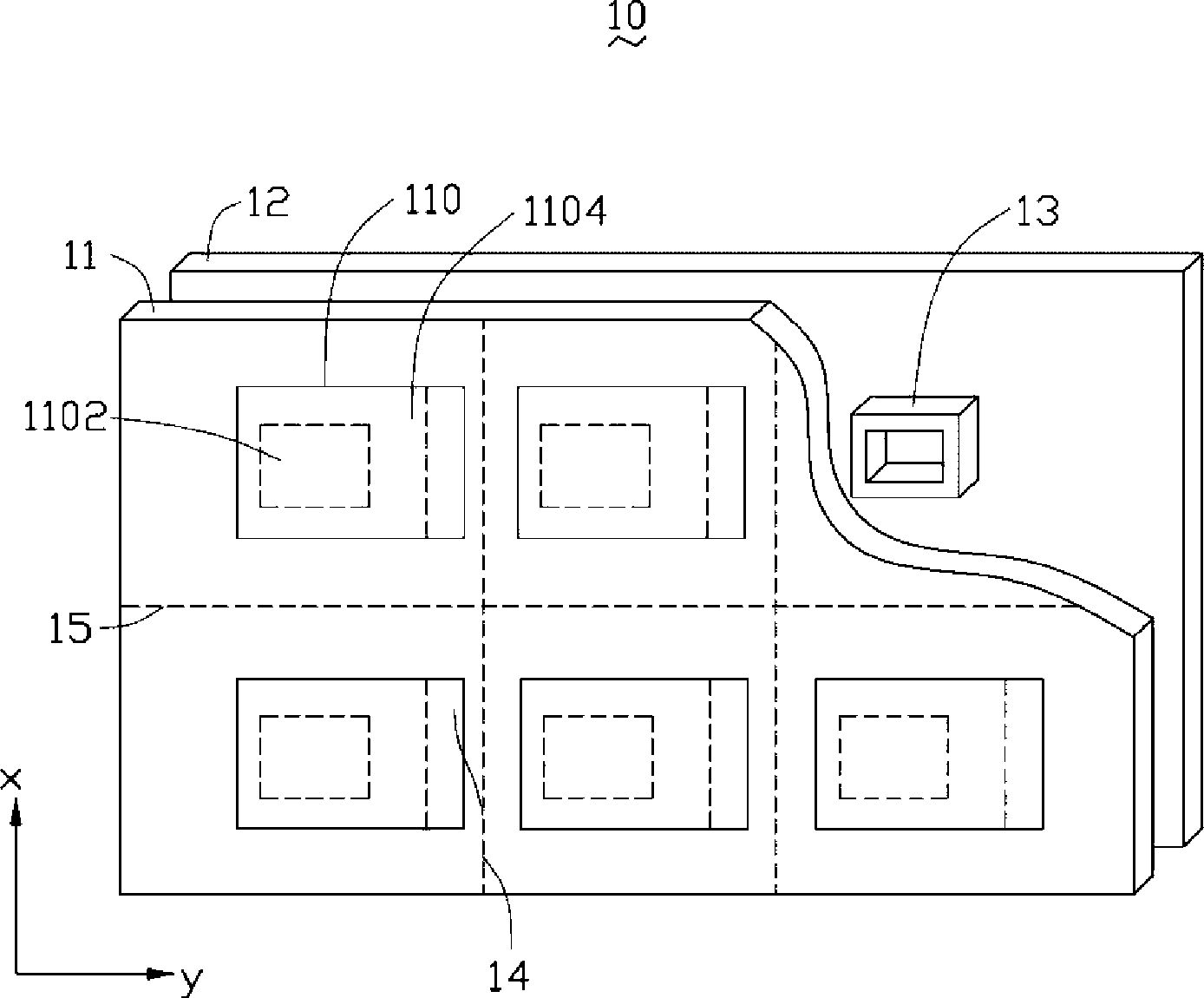
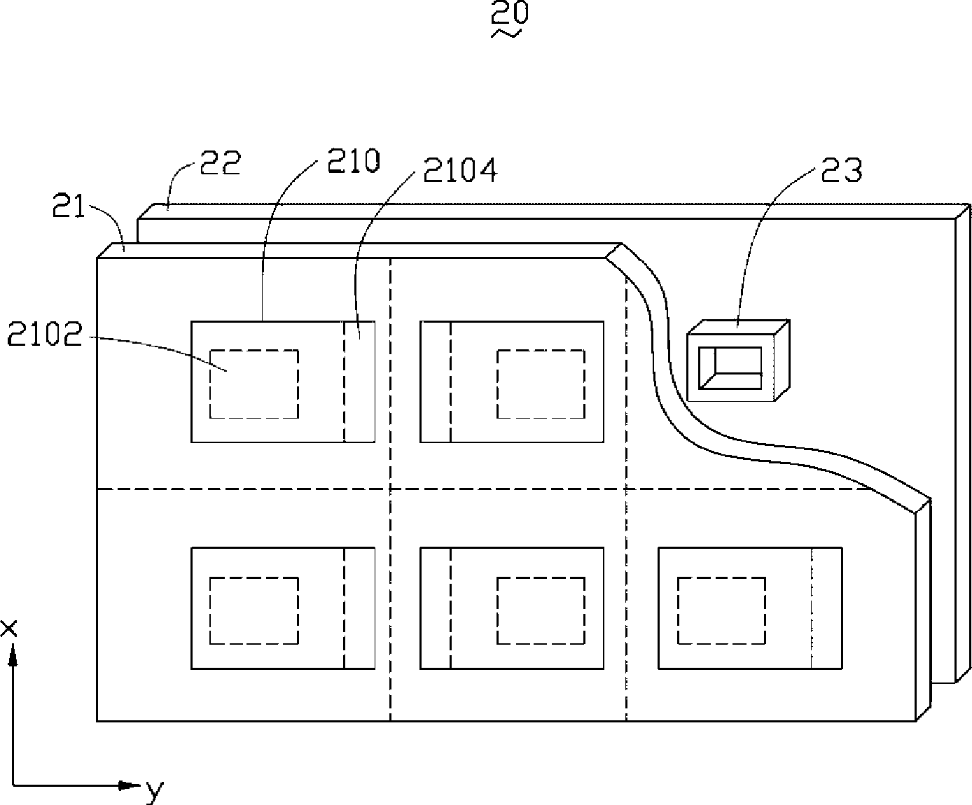
[0014] See figure 2 The liquid crystal panel 20 suitable for high-yield laser cutting provided by the first embodiment of the present invention includes a thin film transistor glass plate 21 , a color filter glass plate 22 and a first sealant 23 . The color filter glass plate 22 is located on one side of the TFT glass plate 21 . The first sealant 23 is located between the TFT glass plate 21 and the color filter glass plate 22 .

[0015] The thin film transistor glass plate 21 includes a plurality of thin film transistor units 210 arranged in an array along the x-axis direction and the y-axis direction. The plurality of thin film transistor units 210 are arranged at intervals, and each thin film transistor unit 210 includes a central area 2102 and a circuit area 2104 located on one side of the central area 2102 . The border of the central area 2102 is bond...


PUM


Abstract

The invention relates to a liquid crystal panel which comprises a film transistor glass plate, first frame glue and a color light filter glass plate which is positioned on one side of the film transistor glass plate, wherein the film transistor glass plate comprises a plurality of film transistor units which are arrayed along a first direction and a second direction which is different from the first direction in an array shape; and the film transistor units are mutually spaced and respectively comprise a central area and a line area which is positioned on one side of the central area. In any two adjacent film transistor units in the first direction, the line area of one film transistor unit is arranged adjacent to the line area of the other film transistor unit, or the central area of one film transistor unit is arranged adjacent to the central area of the other film transistor unit, and boundaries of the central areas are bonded with the color light filter glass plate through the first frame glue.

Description

technical field [0001] The invention relates to a liquid crystal panel, in particular to a liquid crystal panel used in the field of flat panel display manufacture. Background technique [0002] During the manufacturing process of the flat panel display device, it is usually necessary to use a laser scribe (Laser Scribe) to cut a larger-sized panel. [0003] See figure 1 , a liquid crystal panel 10 for laser cutting includes a thin film transistor (Thin Film Transistor, TFT) glass plate 11 and a color filter (Color Filter, CF) glass plate 12 positioned at one side of the thin film transistor glass plate 11 . The thin film transistor substrate 11 includes a plurality of rectangular thin film transistor units 110 , and the thin film transistor units 110 include a central area 1102 and a circuit area 1104 . The plurality of thin film transistor units 110 in the same direction (such as figure 1 shown in the y-direction), that is, from figure 1 From the point of view, the li...

Claims


Application Information

Patent Timeline
IPC IPC(8): G02F1/1362G02F1/1339
Inventor 傅承祖黄俊凯何仁钦周祥瑞张坤旺罗志刚
Owner STATE GRID CORP OF CHINA
Why Eureka
Try Eureka