Conducting wire frame and method for manufacturing same

A manufacturing method and a technology of a lead frame, which are applied in semiconductor/solid-state device manufacturing, semiconductor devices, semiconductor/solid-state device components, etc., can solve the problem of inability to control the thickness ratio at will, the degree of thickness control at will, and the time-consuming manufacturing process. Problems such as labor consumption, to achieve the effect of simplifying production costs and procedures, simplifying complexity, and increasing production speed

Inactive Publication Date: 2009-09-30
I-CHIUN PRECISION IND CO LTD
View PDF3 Cites 6 Cited by
  • Summary
  • Abstract
  • Description
  • Claims
  • Application Information

AI Technical Summary

Problems solved by technology

[0005] The manufacturing methods described in the above three patents all have a shortcoming. It is necessary to process the entire strip first or to purchase a strip of a specific shape (that is, a special-shaped material) before proceeding to the subsequent process.
Additionally, if figure 1 The convex strip 10 of the material strip 1 shown is a long strip, so the entire material strip can only have a thickness ratio, so the thickness cannot be controlled arbitrarily.
Figure 2A The thick copper plate 2 shown requires another processing equipment - milling machine, to carry out the cutting procedure, Figure 2B The joining of the thin copper plate 3 and the thick copper plate 4 also requires a welding process or a pressing process, which is also a function that cannot be provided by punching equipment, and it is time-consuming and labor-intensive to manufacture.
image 3 Shown special-shaped material 5, though need not carry out the processing that makes thick and thin strip, need spend extra purchase cost, and also have the same Figure 1 The disadvantage of the shown strip 1, that is, the thickness ratio cannot be controlled arbitrarily in the same strip

Method used


Image

  • Conducting wire frame and method for manufacturing same
  • Conducting wire frame and method for manufacturing same
  • Conducting wire frame and method for manufacturing same

Examples


Embodiment Construction

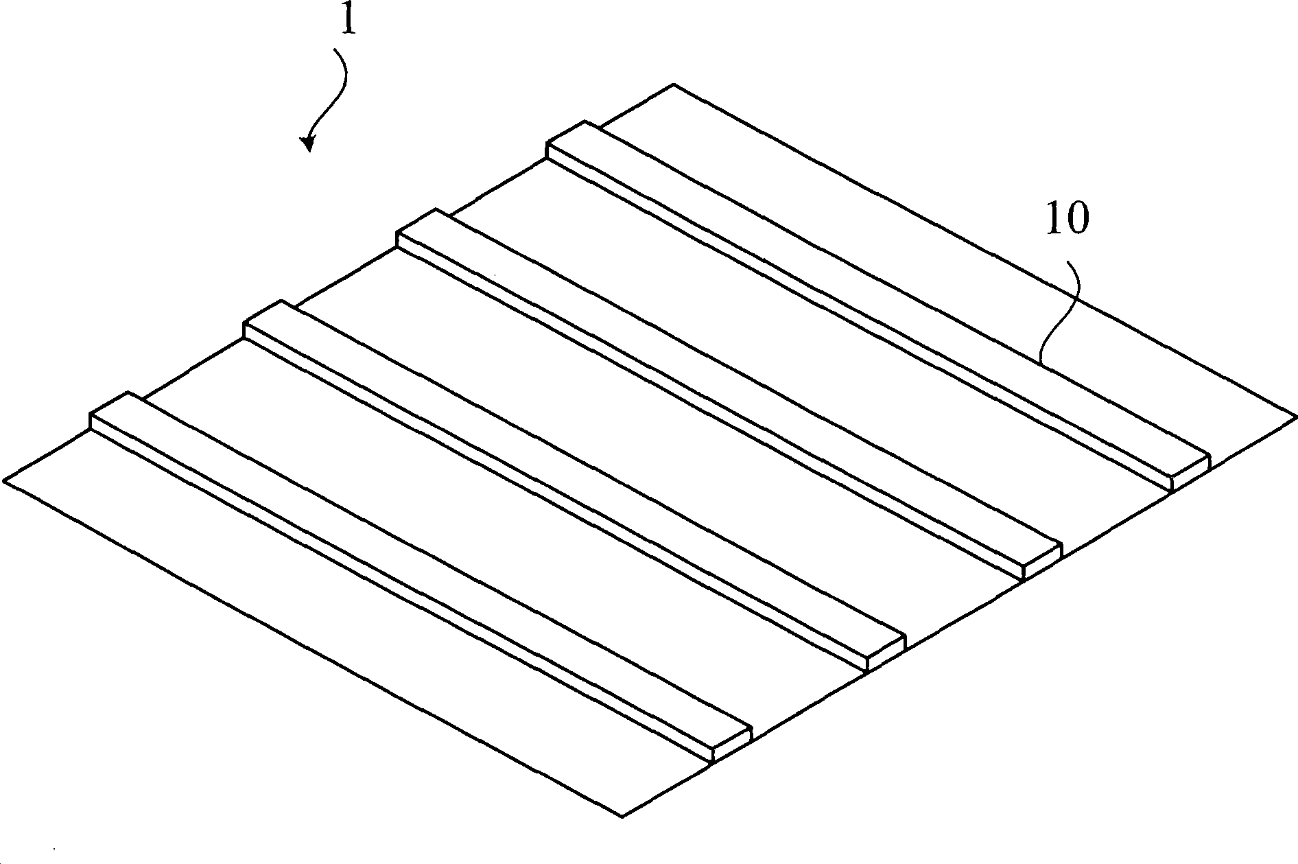
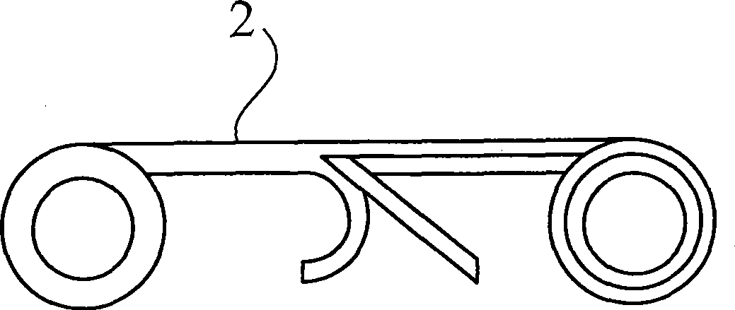
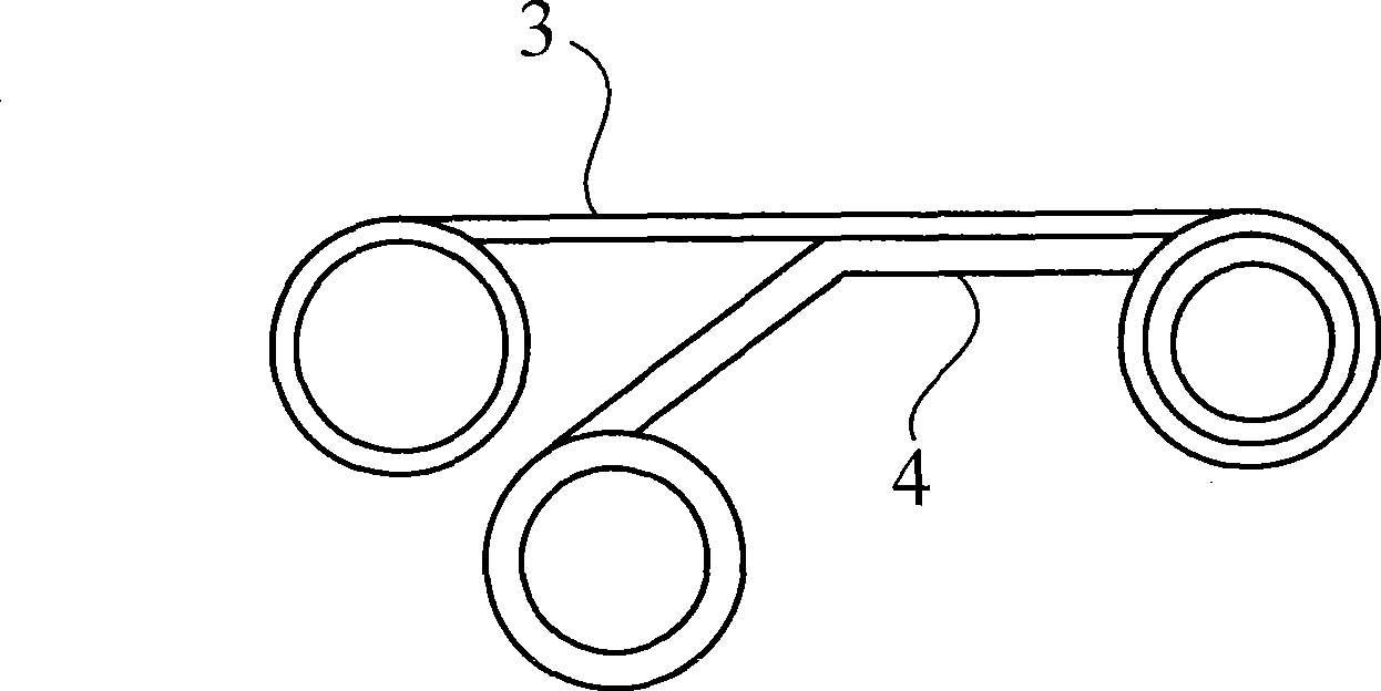
[0024] The present invention utilizes punching method to thin the strip, and then performs punching method to cut out the required components of the lead frame. In this way, the original material strips with uniform thickness can be punched out in a single production process and the thick and thin material strips can be punched out by punching equipment to produce leadframes with bases and brackets with different thicknesses. The detailed lead frame manufacturing method is as follows: Figure 4 shown in the flowchart of the , and to help understand the manufacturing process, please also refer to Figure 5A to Figure 5D manufacturing schematic. Note that, Figure 5A to Figure 5D The slash area in indicates the processing area where the punch punches or punches the strip.

[0025] First, in step S10, the first stamping is carried out, such as Figure 5A As shown, two sets of corresponding through grooves 60 are punched and formed on the material strip 6 . The through groove...


PUM


Abstract

The invention relates to a conducting wire frame and a method for manufacturing the same; in one-time manufacturing flow, a stamping and material extrusion mode is utilized to mold a plurality of regions on each material strip with same sectional area; blocks with different thicknesses are formed in each region through the stamping and material extrusion mode; through the blocks with different thicknesses, a radiation pedestal and a power connection part of the conducting wire frame are formed; then, an insulating shell for covering the radiation pedestal and the power connection part is molded in each region; and further, the conducting wire frame is formed in each region of the material strip. Therefore, the method simplifies the manufacturing flow and reduces the production cost.

Description

technical field [0001] The present invention relates to a lead frame and a manufacturing method thereof, and in particular to a method of first manufacturing a thick and thin material strip and then making a lead frame. Background technique [0002] Due to the increasing demand for high-brightness lighting, the general practice is to package multiple light-emitting chips on a lead frame, and due to the small size of the light-emitting chips and the small distance between them, the heat density generated is very high. In order to solve the heat dissipation problem of the lead frame, the most direct method is to connect the lead frame to a heat dissipation base, or embed and inject the heat dissipation base and the bracket together, and then place the light-emitting chip on the heat dissipation base to improve heat dissipation efficiency. [0003] However, this method requires additional mold opening to make the heat dissipation base, and also needs to carry out bonding proces...

Claims


Application Information

Patent Timeline
Patent Type & Authority Applications(China)
IPC IPC(8): H01L21/48H01L23/495H01L33/00
CPCH01L2224/48091H01L2224/48247
Inventor 朱新昌
Owner I-CHIUN PRECISION IND CO LTD
Why Eureka
Try Eureka