Chip-component-mounted device and semiconductor device

A mounting body, semiconductor technology, applied in the direction of semiconductor devices, semiconductor/solid-state device manufacturing, semiconductor/solid-state device components, etc., can solve the problems of low connection reliability, weak connection strength, poor connection strength, etc., to increase the contact area, The effect of stable connection strength, stable position and inclination

Inactive Publication Date: 2005-12-14
NEC ELECTRONICS CORP
View PDF1 Cites 2 Cited by
  • Summary
  • Abstract
  • Description
  • Claims
  • Application Information

AI Technical Summary

Problems solved by technology

If the connection strength is weak, due to the impact of the assembly process (for example: wire bonding, resin sealing process) after the chip component 102 is mounted, or the temperature change (such as reflow) around the assembled product, the electrodes of the chip component 102 may be damaged. The electrical connection between part 102a and the pad part 101a of the printed wiring board 101 (or the lead part on the lead frame) will be disconnected, and the resistance will increase due to the deterioration of the strength of the joint part.
[0006] The connection strength of conductive adhesive 103 is inferior to that of solder, so the connection reliability is lower than that of solder

Method used


Image

  • Chip-component-mounted device and semiconductor device
  • Chip-component-mounted device and semiconductor device
  • Chip-component-mounted device and semiconductor device

Examples


Embodiment approach 1

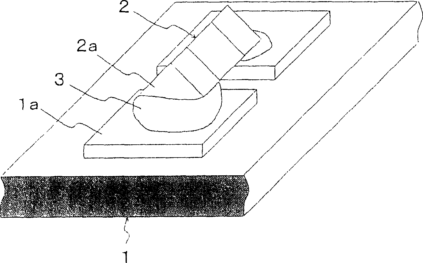
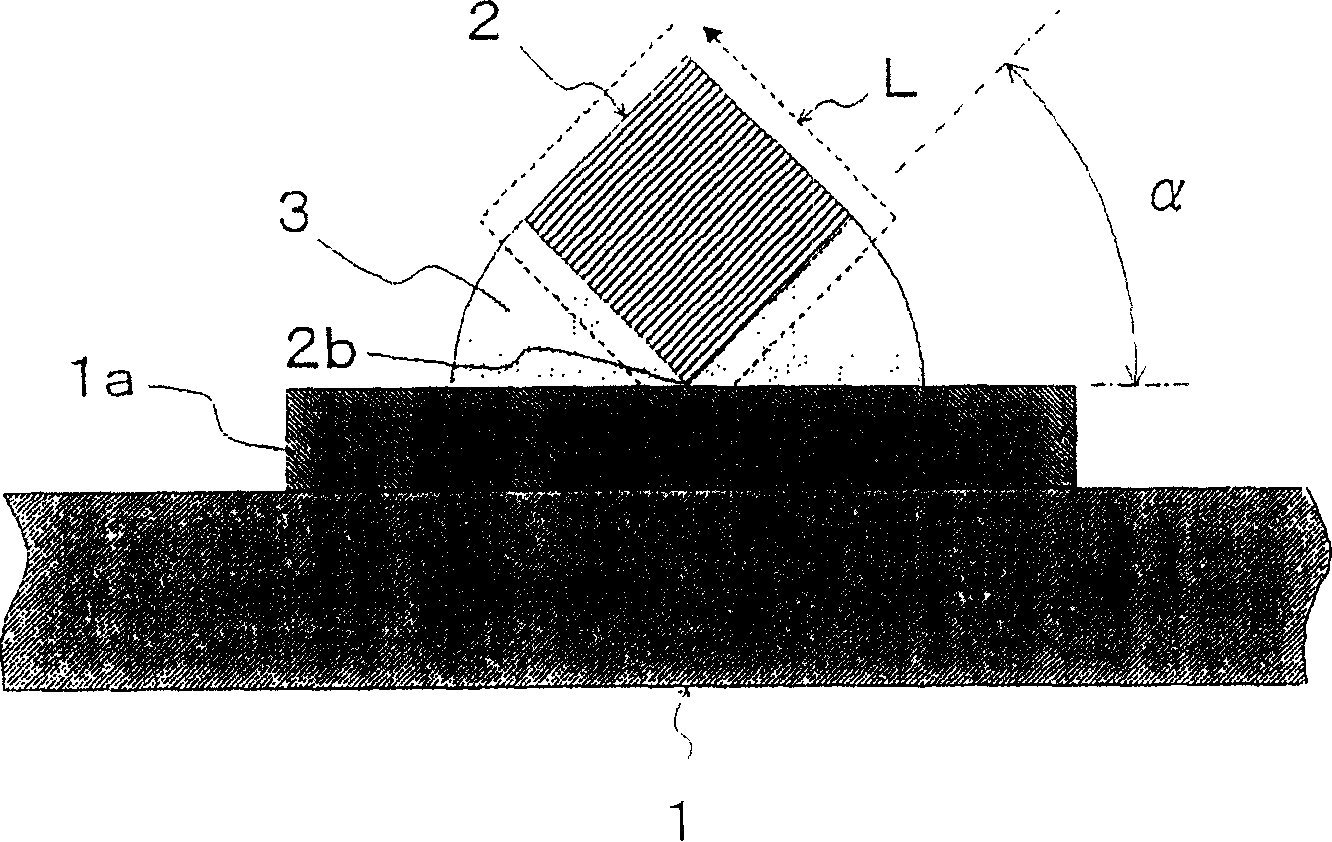
[0026] In Embodiment 1, on the two land portions 1a (connected portions) of the printed wiring board 1 on which a semiconductor element (not shown) is mounted, the chip component 2 is arranged across the two land portions 1a, and the chip component The corner portion 2b of 2 is mounted facing the land portion 1a side. The pad portion 1 a and the corresponding electrode portion 2 a are physically and electrically connected by the conductive adhesive 3 . The pad portion 1a of the printed wiring board 1 is a conductive pad formed on the surface of the wiring (not shown) of the printed wiring board 1, and is made of noble metal such as Au. The corresponding land portions 1 a are arranged at predetermined intervals. The chip component 2 is an electronic component such as a capacitor, a resistor, or an inductor, and is a chip-shaped electronic component having at least a corner portion 2b, and has electrode portions 2a at both ends. The electrode portion 2a of the chip component 2...

Embodiment approach 2

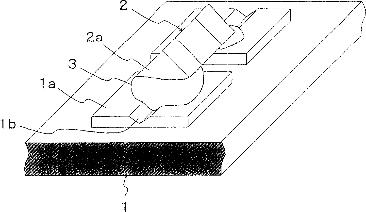
[0030]In Embodiment 2, as in Embodiment 1, on two pad portions 1a (connected portions) of a printed wiring board 1 on which a semiconductor element (not shown) is mounted, a chip component 2 straddles between the two pad portions 1a. However, it is arranged so that the corner portion 2b of the chip component 2 is mounted facing the pad portion 1a side. The pad portion 1 a and the corresponding electrode portion 2 a are physically and electrically connected by the conductive adhesive 3 . The pad portion 1a of the printed wiring board 1 is a conductive pad formed on the surface of the wiring (not shown) of the printed wiring board 1, and is made of noble metal such as Au. The corresponding land portions 1 a are arranged at predetermined intervals. The chip component 2 is an electronic component such as a capacitor, a resistor, or an inductor, and is a chip-shaped (for example, rectangular parallelepiped, cubic) electronic component having at least corners 2b, and has electrode ...


PUM


Abstract

The present invention provides a chip component package and a semiconductor device capable of suppressing short circuits with adjacent pads or components even if the amount of the conductive adhesive is increased to increase the contact area between the chip component and the conductive adhesive. . A chip component mounting body in which a chip component (2) is mounted on a printed wiring board (1) through a conductive adhesive (3), is characterized in that the chip component has a corner (2b), and the corner The ridgeline of the part is arranged toward the pad part (1a) side of the printed wiring board, and the angle (α) formed by the surface adjacent to the ridgeline of the corner part of the chip component and the surface of the pad part becomes an acute angle. is carried.

Description

technical field [0001] The present invention relates to a chip component package and a semiconductor device in which chip components are mounted on a printed wiring board or a lead frame, and particularly relates to a chip component package and a chip component package capable of suppressing short circuits with adjacent pad portions (or lead portions) and components. semiconductor device. Background technique [0002] In recent years, as high-density packaging of semiconductor devices in which semiconductor elements are mounted on printed wiring boards (or lead frames) is progressing, the importance of package-type semiconductor devices in which chip components are mounted is also increasing. For example, chip components such as bypass capacitors for stabilizing power supply, capacitors for stabilizing circuit operation, load resistors, and inductors are arranged around the semiconductor element. Also, in many package-type semiconductor devices, semiconductor elements and c...

Claims


Application Information

Patent Timeline
Patent Type & Authority Applications(China)
IPC IPC(8): H01L21/60H01L23/48H05K1/02H05K1/11H05K1/18H05K3/32
CPCH01L2924/0002H05K1/111H05K3/321H05K2201/09745H05K2201/10484H05K2201/10636Y02P70/50H01L2924/00H01L23/12
Inventor 中泽大望
Owner NEC ELECTRONICS CORP
Why Eureka
Try Eureka