Semiconductor device and method for manufacturing semiconductor device

A manufacturing method and semiconductor technology, applied in semiconductor/solid-state device manufacturing, semiconductor devices, transistors, etc., can solve the problems of wiring pattern lengthening, reducing wiring pattern resistance, etc., to prevent interface diffusion, excellent electrical characteristics, and high transparency Effect

Inactive Publication Date: 2009-10-21
TOHOKU UNIV +2
View PDF5 Cites 0 Cited by
  • Summary
  • Abstract
  • Description
  • Claims
  • Application Information

AI Technical Summary

Problems solved by technology

Furthermore, when enlarging the display device, the wiring pattern itself will become longer, so it is necessary to reduce the resistance of the wiring pattern.

Method used


Image

  • Semiconductor device and method for manufacturing semiconductor device
  • Semiconductor device and method for manufacturing semiconductor device
  • Semiconductor device and method for manufacturing semiconductor device

Examples


Embodiment

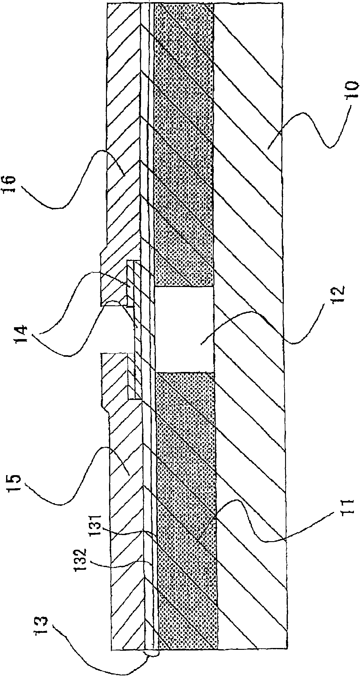
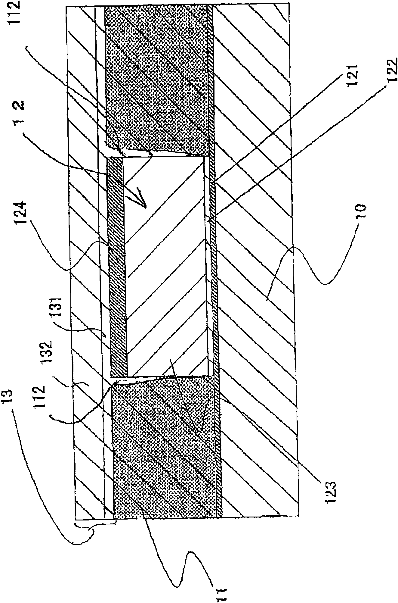
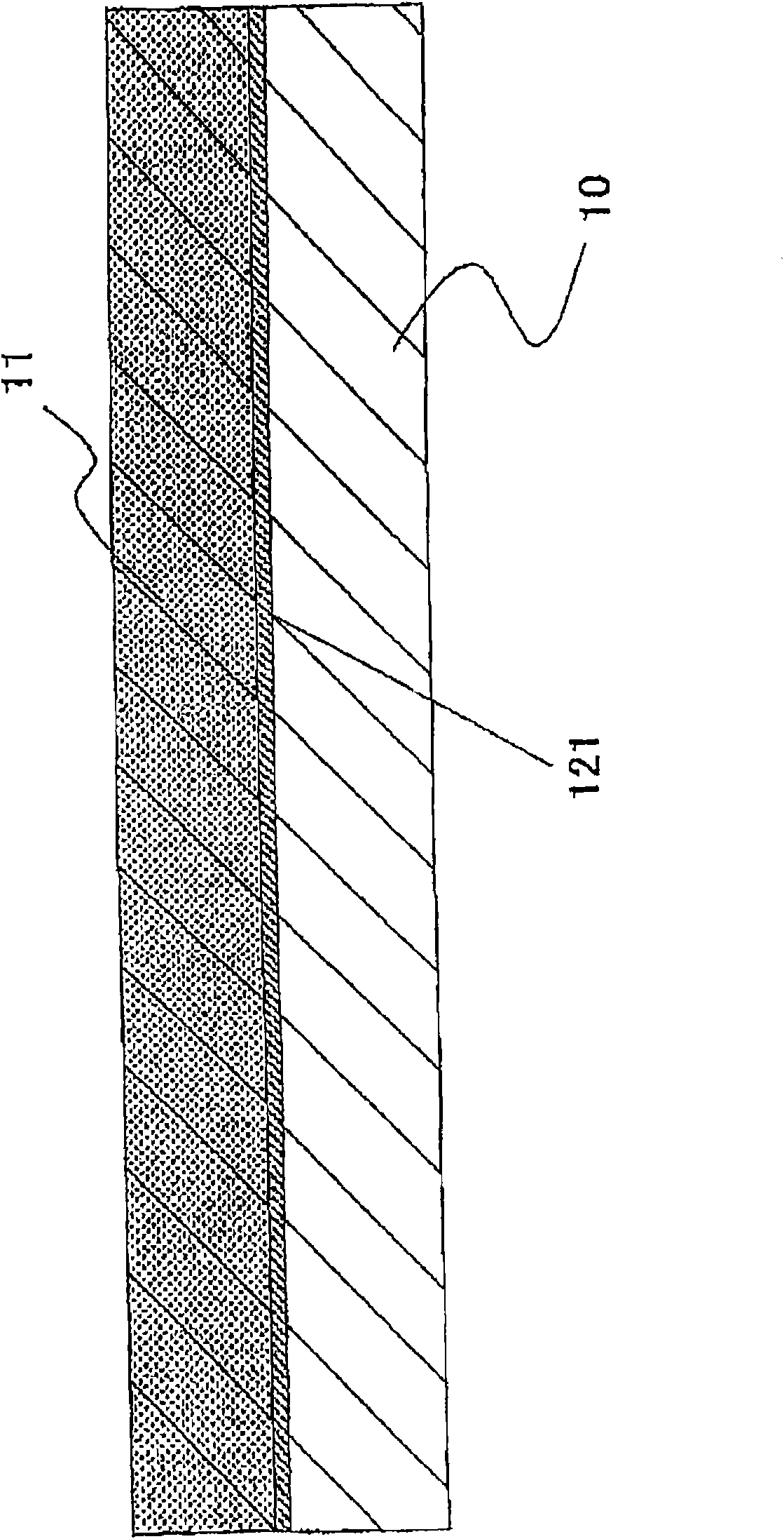
[0096] Next, the method of forming the thin film transistor according to the embodiment of the present invention described above will be described using the drawings. Figure 3 ~ Figure 7 It is a schematic diagram illustrating the manufacturing method of the thin film transistor of this embodiment in the order of steps. First, refer to image 3 , The glass substrate 10 is prepared as a substrate. This substrate is a large substrate capable of forming a large screen of 30 inches or more. The substrate was treated in a 0.5 vol% hydrofluoric acid aqueous solution for 10 seconds, and the surface was washed with pure water, thereby washing and removing surface contamination.

[0097] Then, sodium hydroxide was added to pure water to obtain an aqueous solution whose pH was controlled at 10, and the silane coupling agent, namely aminopropylethoxysilane, was dissolved at a concentration of 0.1% by volume in the aqueous solution to form such a silane coupling agent solution. The glass subst...


PUM


Abstract

Disclosed is a thin-film transistor (TFT) having a gate insulating film excellent in transparency and planarity. Also disclosed is a method for manufacturing such a thin-film transistor. A transparent insulating film (131) composed of an oxide represented by RxMOy is formed as a gate insulating film arranged between a gate electrode and a semiconductor layer. The transparent insulating film (131) is made of a coating agent which is composed of one mixed liquid obtained by dissolving or dispersing a condensate, which is obtained by subjecting a compound represented by RxMXm-x to a hydrolysis-condensation reaction, in an organic solvent, water or their mixed solvent, or alternatively a coating agent which is obtained by mixing two or more of such mixed liquids.

Description

Technical field [0001] The present invention relates to semiconductor devices, and more particularly to thin film transistors (TFTs) and manufacturing methods thereof. Background technique [0002] Generally, display devices such as liquid crystal display devices, organic EL devices, and inorganic EL devices are formed by sequentially forming a film on a substrate having a flat one main surface and patterning conductive patterns such as wiring patterns and electrode patterns. Then, a film is sequentially formed on the elements constituting the electrode film and the display device, and various necessary films and the like are patterned to fabricate the display device. [0003] In recent years, there has been a strong demand for large-scale display devices of this type. In order to obtain a large-scale display device, it is necessary to form more display elements with high precision on the substrate, and to electrically connect these elements with the wiring pattern. At this time,...

Claims


Application Information

Patent Timeline
Patent Type & Authority Applications(China)
IPC IPC(8): H01L29/786H01L21/336
CPCH01L27/1214H01L29/4908H01L29/78639H01L27/1292H01L29/42384H01L29/78603
Inventor 大见忠弘杉谷耕一小池匡番场昭典小林章洋绵贯耕平
Owner TOHOKU UNIV
Why Eureka
Try Eureka