Sull transistor with etching barrier layer and preparation method thereof

A technology for etching barrier layers and oxide films, used in transistors, semiconductor/solid-state device manufacturing, semiconductor devices, etc., can solve problems such as easy leakage, and achieve the effect of avoiding influence and ensuring electrical properties

Inactive Publication Date: 2009-11-04
AU OPTRONICS CORP
View PDF0 Cites 29 Cited by
  • Summary
  • Abstract
  • Description
  • Claims
  • Application Information

AI Technical Summary

Problems solved by technology

Although this process can avoid the problems described in the first structure, in the process step of etching the etching stopper layer 250', the parts of the insulat

Method used


Image

  • Sull transistor with etching barrier layer and preparation method thereof
  • Sull transistor with etching barrier layer and preparation method thereof
  • Sull transistor with etching barrier layer and preparation method thereof

Examples


Embodiment Construction

[0016] An oxide thin film transistor with an etching stopper layer and a manufacturing method thereof provided by the present invention will be described in detail below with reference to the accompanying drawings.

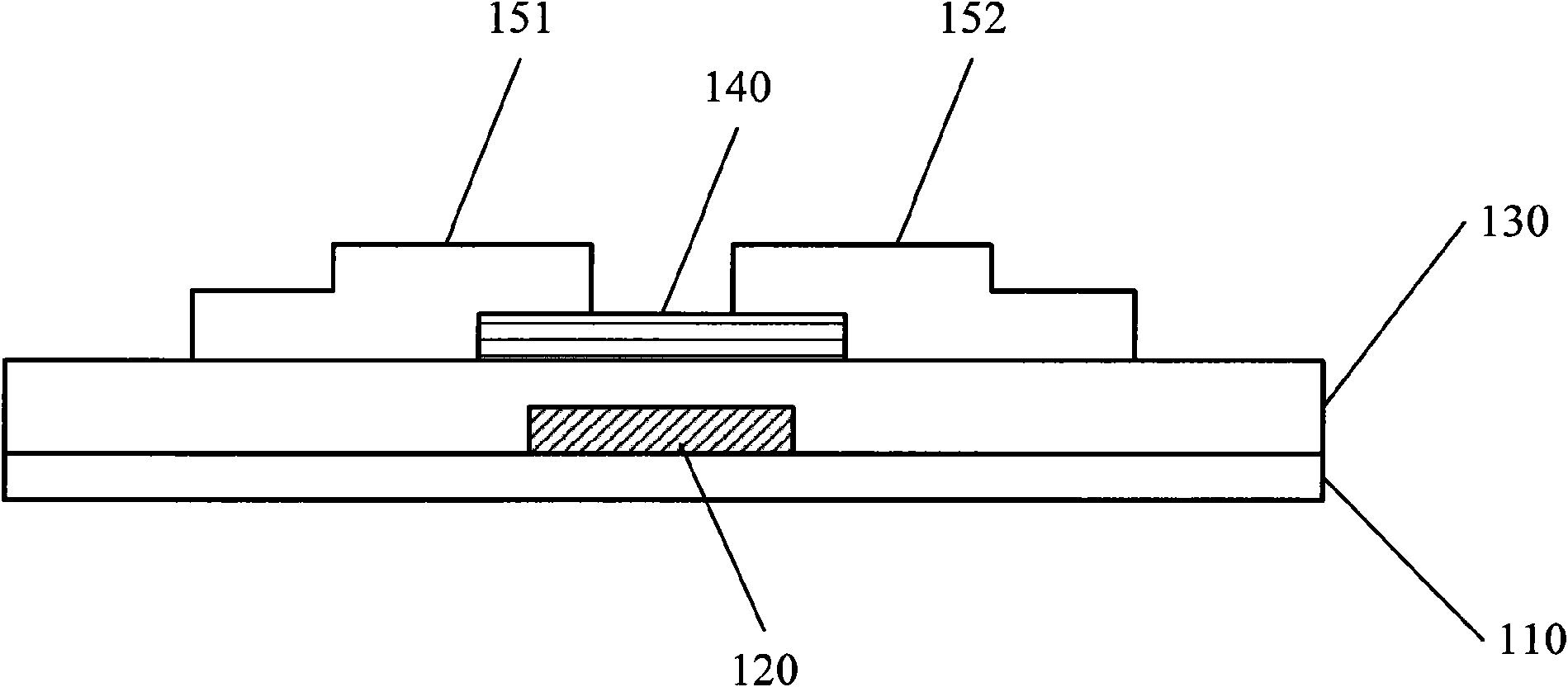
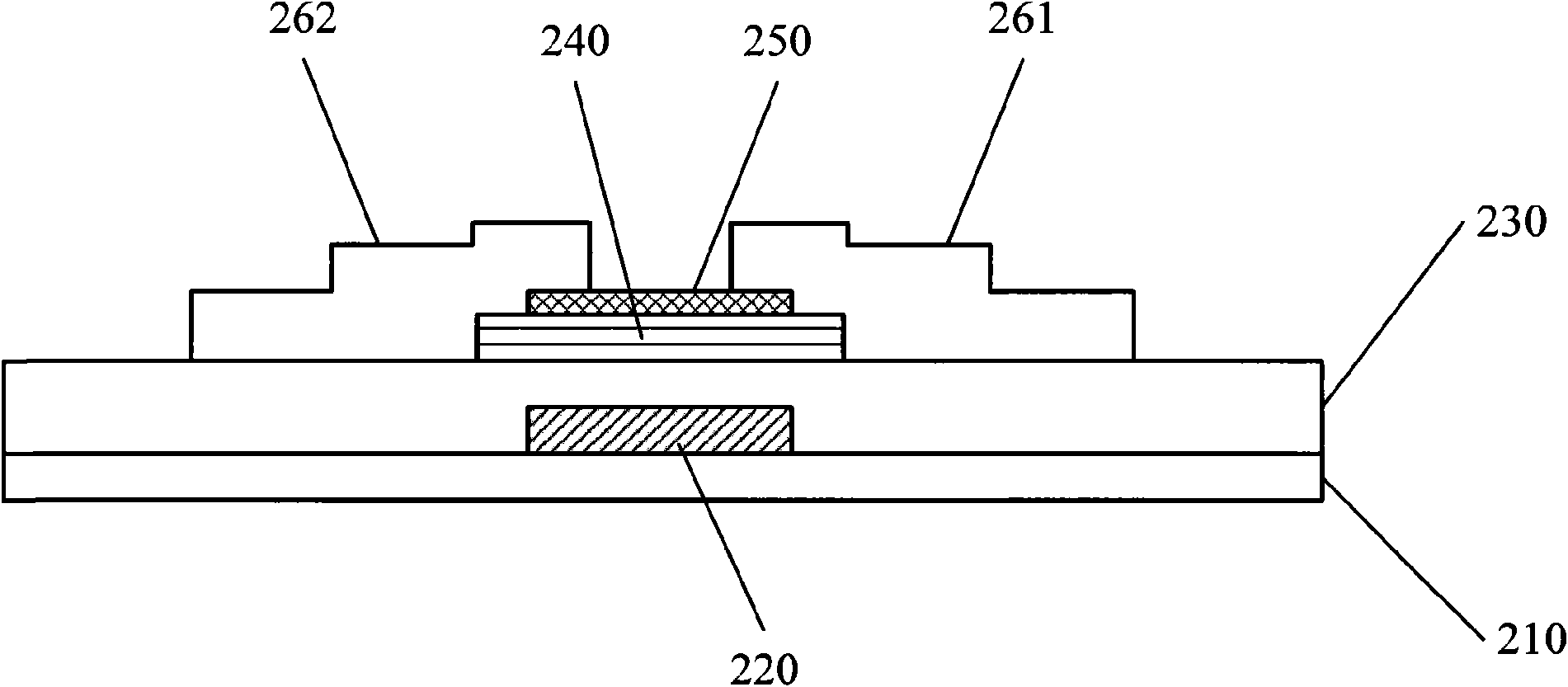
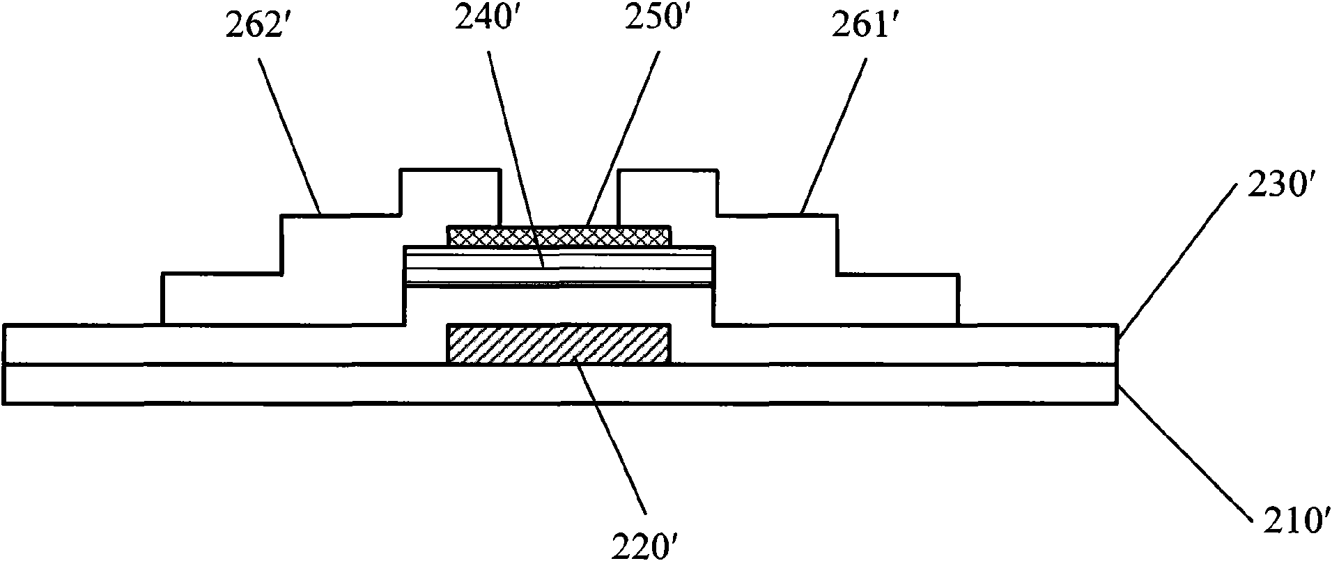
[0017] attached Figure 4 It is a structural schematic diagram of the thin film transistor described in this specific embodiment, including: a substrate 310; a gate 320, the gate 320 is arranged on the surface of the substrate 310; an insulating layer 330, the insulating layer 330 covers the surface of the gate 320 Covering all; the conductive channel 340 , the conductive channel 340 is disposed on the surface of the insulating layer 330 away from the gate 320 , and corresponds to the position of the gate 320 . The material of the conductive channel 340 is an oxide semiconductor, preferably an oxide material (InGaZnO) containing metal indium, gallium and zinc.

[0018] The structure described in this specific embodiment further includes an etching barrier layer 3...


PUM


Abstract

The invention relates to a sull transistor with an etching barrier layer, which comprises a substrate, a grid, an insulating barrier, an electric conduction channel, a source electrode and a drain electrode; the electric conduction channel is arranged on the surface of the insulating barrier far from the grid and is corresponding to the grid; the etching barrier layer wholly covers the electric conduction channel and the surface of the insulating layer and is provided with a through hole on a position corresponding to the surface of the electric conduction channel; the source electrode and the drain electrode are connected with the electric conduction channel by the through hole in the etching barrier layer. The invention also provides a method for preparing the transistor. The invention has the advantages that the etching barrier layer is adopted for wholly covering the insulating layer and the surface of the electric conduction channel, the through hole is only manufactured on a position needing the connection forming, thus avoiding the influence of a plasma etching technique on the insulating layer and the electric conduction channel and ensuring the stability of the electrical property of the sull transistor.

Description

【Technical field】 [0001] The invention relates to the field of semiconductor devices, in particular to an oxide thin film transistor with an etching stopper layer and a preparation method thereof. 【Background technique】 [0002] Oxide thin film transistors are an emerging research topic in recent years, and many academic institutions and companies have invested in research and development, mainly because it has many excellent characteristics, for example, because these metal oxides have special carrier transport Characteristics, high carrier mobility can be achieved in the amorphous state, and because it is in the amorphous state, the uniformity will be better than that of general polycrystalline semiconductors. Additionally, since it can be deposited at relatively low or even room temperature, it can be applied to a wide variety of substrates. [0003] The bottom gate (Bottom Gate) structure is an oxide thin film transistor structure commonly used at present, including a b...

Claims


Application Information

Patent Timeline
IPC IPC(8): H01L29/786H01L29/06H01L29/10H01L21/336H01L21/314
Inventor 谢信弘
Owner AU OPTRONICS CORP
Why Eureka
Try Eureka