

Polysilicon membrane forming method and polysilicon gate forming method
A polysilicon film and polysilicon layer technology is applied in the growth of polysilicon materials, chemical instruments and methods, crystal growth and other directions, which can solve the problem that the polysilicon film cannot take into account the flatness and interface quality, etc., to improve the electrical properties and crystal grains. Size, smooth transition effect
Inactive Publication Date: 2010-11-10
SEMICONDUCTOR MANUFACTURING INTERNATIONAL (BEIJING) CORP
View PDF1 Cites 0 Cited by
- Summary
- Abstract
- Description
- Claims
- Application Information
AI Technical Summary
Problems solved by technology
The invention provides a method for forming a polysilicon thin film and a polysilicon grid, so as to improve the phenomenon that the existing polysilicon thin film formation method cannot meet the requirements of flatness and interface quality, and improve the formation quality of the polysilicon grid
Method used
View moreImage
Smart ImageViewing Examples


Examples
no. 1 example
no. 2 example
Login to View More PUM
 Abstract
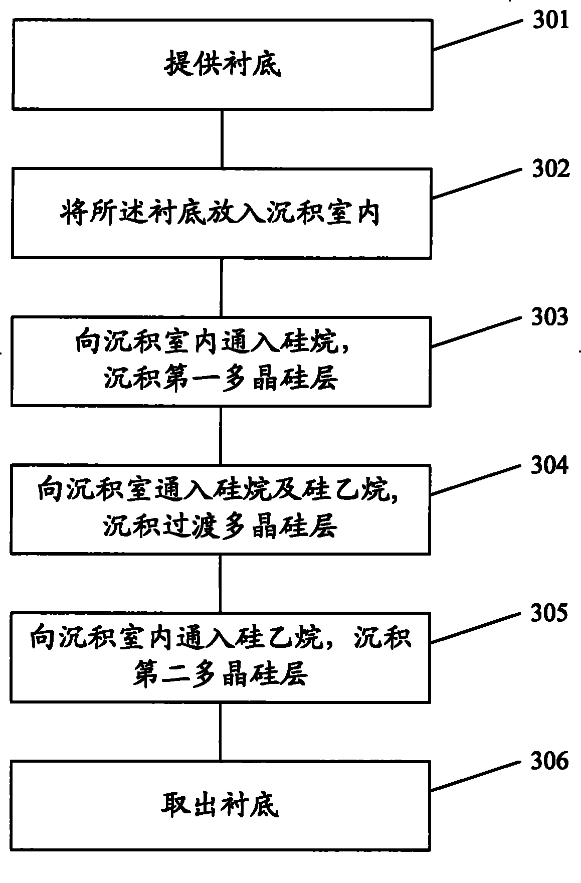
The invention discloses a polysilicon membrane forming method comprising the following steps: providing a substrate; putting the substrate in a settling chamber; leading silane into the settling chamber and settling a first polycrystalline silicon layer on the substrate; leading silane and silicoethane to the settling chamber and settling a transition polycrystalline silicon layer on the first polycrystalline silicon layer; leading silicoethane to the settling chamber and settling a second polycrystalline silicon layer on the transition polycrystalline silicon layer; and taking out the substrate. The invention also correspondingly discloses a method for forming gates by utilizing the polysilicon membrane. The polysilicon membrane formed by the method not only satisfies the requirements ofplaneness and interface quality, but also enables the transition of each layer of the polysilicon membrane to be more stable, thereby further enhancing the forming quality of the polysilicon membrane.
Description
Method for forming polysilicon film and polysilicon gate technical field The invention relates to the technical field of semiconductor manufacturing, in particular to a method for forming a polysilicon thin film and a polysilicon gate. Background technique With the rapid development of ultra-large-scale integrated circuits, the integration of chips is getting higher and higher, and the size of components is getting smaller and smaller. The various effects caused by the high density and small size of devices have an increasing impact on the results of semiconductor process manufacturing. Outstanding, new process improvements are often required for small-scale devices. Taking the manufacture of polysilicon gates as an example, when the size of the device is reduced, small-sized devices made with the gate of the original large-sized device tend to have poor gate leakage current performance. The device is no longer suitable and needs to be improved and optimized. Metal Oxid...
Claims
Login to View More Application Information
Patent Timeline
 Patent Type & AuthorityPatents(China)
IPC IPC(8): H01L21/205H01L21/28H01L21/285H01L21/336C30B28/14
Inventor何永根
OwnerSEMICONDUCTOR MANUFACTURING INTERNATIONAL (BEIJING) CORP