Dry etching method for removing silicon nitride film

A technology of silicon nitride thin film and dry etching, which is applied in the direction of electrical components, semiconductor/solid-state device manufacturing, circuits, etc., can solve the problems of affecting the electrical performance of semiconductor devices, damage, and the inability to deposit gate oxide layers, etc., to achieve reduction The chance of bombardment, reducing the severity, and reducing the effect of potential difference

Inactive Publication Date: 2011-10-05
SEMICON MFG INT (SHANGHAI) CORP
View PDF0 Cites 0 Cited by
  • Summary
  • Abstract
  • Description
  • Claims
  • Application Information

AI Technical Summary

Problems solved by technology

[0004] After adopting the above method, it is found that the gate oxide layer 24 of other semiconductor devices produced is smaller than the expected thickness, and in severe cases, the thickness is 10 Angstroms less than the expected thickness, which seriously affects the electrical performance of the semiconductor device.
The study found that the silicon lattice on the surface of the silicon substrate was damaged by the intense bombardment of the plasma during the above-mentioned dry etching step, so that the gate oxide layer of other devices could not be deposited in the damaged area

Method used


Image

  • Dry etching method for removing silicon nitride film
  • Dry etching method for removing silicon nitride film

Examples


Embodiment Construction

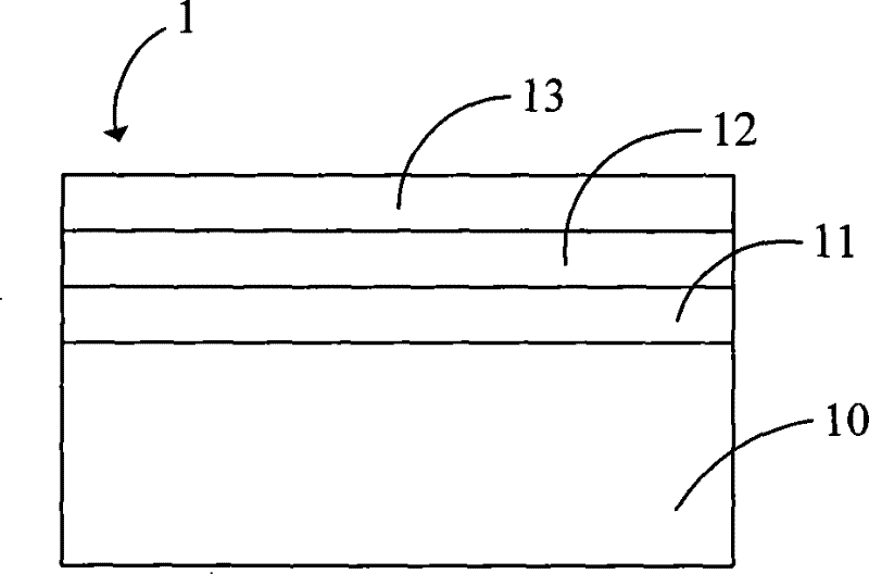
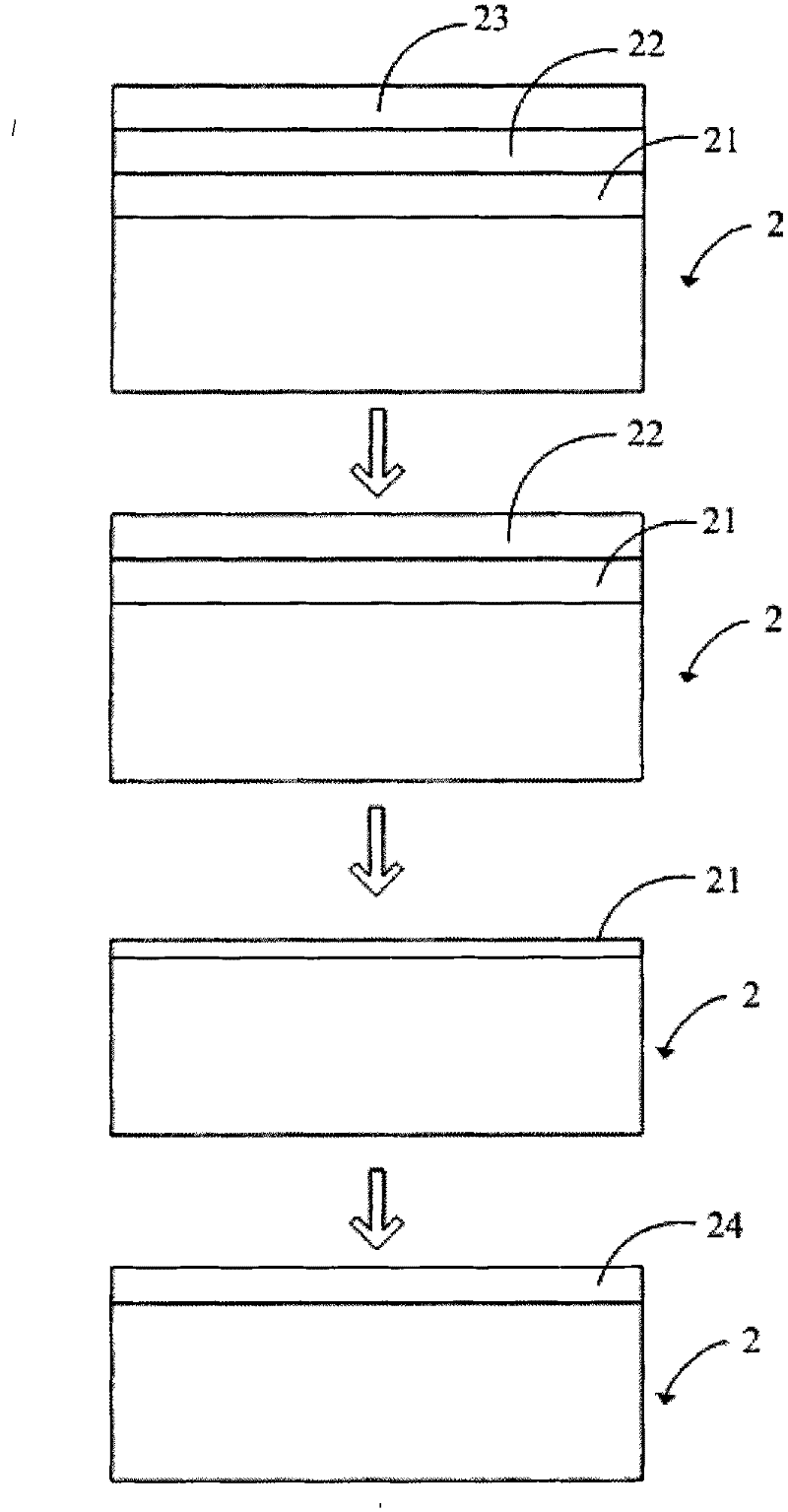
[0010] One embodiment of the dry etching method for removing silicon nitride film provided by the present invention will be described in detail below with reference to the accompanying drawings, in order to further understand the technical scheme, purpose and beneficial effects of the invention. . see figure 2 For the sake of concise description, in this embodiment, the etching of the silicon nitride film, the oxide film where the gate oxide and the inter-electrode oxide are located is referred to as the ONO etching process.

[0011] The dry etching method provided by the invention is applied in the ONO etching process. The dry etching method is used to remove the silicon nitride film 22 in the non-flash MOS tube region, and is performed in a process chamber. The upper and lower sides of the plasma region of the processing chamber have an upper substrate and a lower substrate. The upper plate is connected to the source power to excite the gas input into the process chamber...


PUM


Abstract

The invention discloses a dry etching method for removing a silicon nitride film and relates to the etching technology in the field of semiconductor manufacture. The dry-method etching method is carried out in a processing procedure chamber, and the electric potential difference of an upper substrate and a lower substrate respectively arranged at both sides of a plasma region in the processing procedure cavity is smaller than 300 volts. Compared with the prior art, the dry etching method for removing the silicon nitride film reduces the electric potential difference of the plasma region to greatly decrease the bombing possibility of plasma bodies on a wafer silicon substrate and optimize the subsequent technologies.

Description

technical field [0001] The invention relates to a dry etching method for manufacturing a semiconductor non-volatile memory device, in particular to a dry etching method for removing a silicon nitride film. Background technique [0002] Flash memory is a non-volatile memory that can store charge even when the system is powered off. The storage unit of the flash memory is a MOS tube, but its structure is slightly different from that of a general MOS tube. The structure of the flash MOS tube is as follows figure 1 As shown, the structure of the flash memory MOS transistor region 1 includes a silicon substrate 10, a gate oxide layer 11, a floating gate 12, an inter-electrode oxide layer 13 and a control gate (not shown) from bottom to top. The floating gate 12 is made of silicon nitride (Si 3 N 4 ) film to store charge. Both the gate oxide layer 11 and the inter-electrode oxide layer 13 are silicon dioxide (SiO 2 )film. [0003] Generally, a variety of semiconductor devic...

Claims


Application Information

Patent Timeline
Patent Type & Authority Patents(China)
IPC IPC(8): H01L21/311
Inventor 黄敬勇钟鑫生朱海波方文强
Owner SEMICON MFG INT (SHANGHAI) CORP
Why Eureka
Try Eureka