Inner cavity type multiple-active region photon crystal vertical cavity surface transmission semiconductor laser device
A vertical cavity surface emission and photonic crystal technology, applied in the field of optoelectronics, can solve the problems of poor thermal stability of devices, difficulty in controlling small oxidation holes, low single-mode output power, etc., to achieve improved thermal stability and narrow line width , the effect of emphasizing the modulation characteristics
Inactive Publication Date: 2011-01-05
BEIJING UNIV OF TECH
View PDF0 Cites 0 Cited by
- Summary
- Abstract
- Description
- Claims
- Application Information
AI Technical Summary
Problems solved by technology
Such a small oxide pore size will inevitably lead to a large series resistance
At the same time, a large series resistance will inevitably generate a lot of heat, which will deteriorate the thermal stability of the device.
It is difficult to control the process of making small oxidation holes 9
The smaller oxidation hole 9 makes the effective light-emitting area smaller and the single-mode output power is low
Method used
View moreImage
Smart ImageViewing Examples

Examples
Embodiment Construction
Login to View More PUM
 Abstract
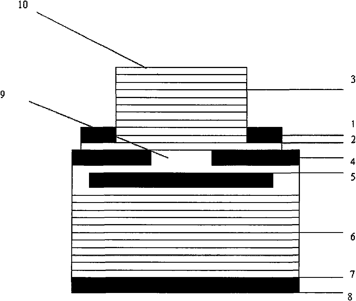
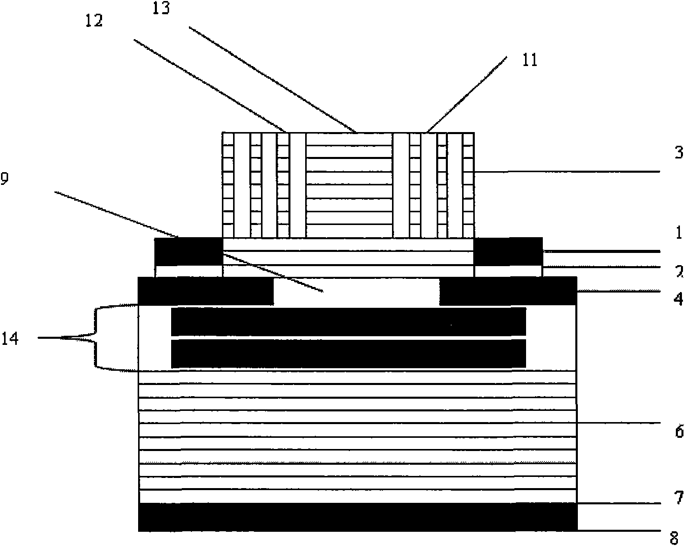
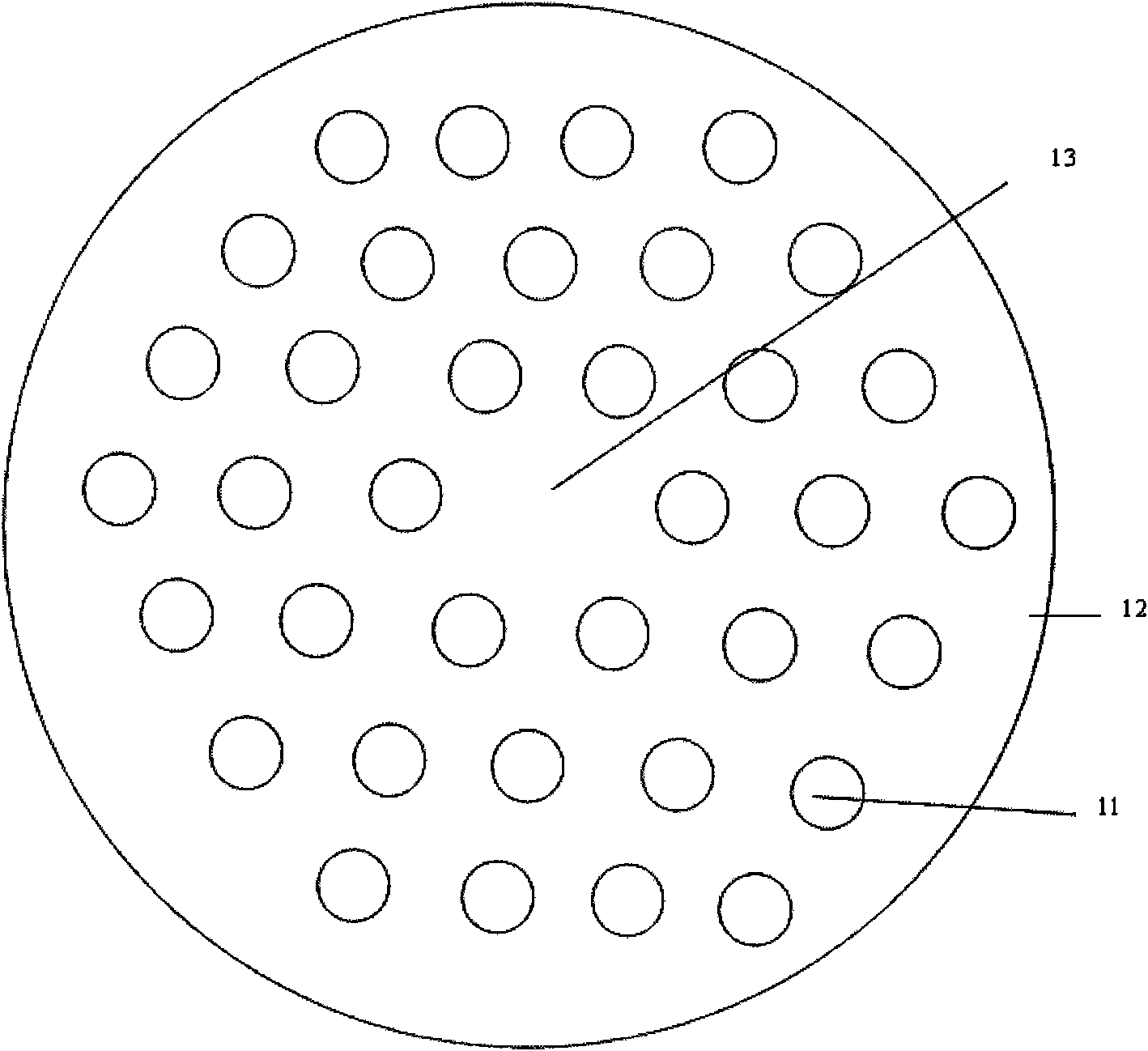
The invention relates to an inner cavity type multiple-active region photon crystal vertical cavity surface transmission semiconductor laser device, belonging to the semiconductor photoelectron field.The common oxidation limiting vertical cavity surface transmission semiconductor laser device has problems of multiple-transverse module laser shooting, low single module output power, large threshold current and large series resistance and so on. The invention adopts the multiple-active region structure on the active region of the device, meanwhile leads the defect type photon crystal structureinto DBR on the vertical cavity surface transmission semiconductor laser device, the inner cavity type multiple-active region photon crystal vertical cavity surface transmission semiconductor laser device with dozens of micrometres of single module operation oxidation bore diameter, dozens of mws of single module power, dozens of Ohms of series resistances and more than 40 dbs of side module inhibition can be obtained by optimizing the photon crystal period, the air bore diameter, the etching depth, the device diameter and the oxidation bore diameter and so on reasonably.
Description
Intra-cavity multi-active area photonic crystal vertical cavity surface-emitting semiconductor laser technical field The invention belongs to the technical field of optoelectronics, and in particular relates to the design and manufacture of a novel vertical cavity surface emitting semiconductor laser. Background technique Vertical cavity surface emitting laser (VCSEL) has the advantages of low threshold current, dynamic single longitudinal mode operation, small divergence angle, circular symmetric beam, high modulation bandwidth, easy two-dimensional integration, etc., and can be widely used in optical communication, optical storage and optical display and other fields. Common oxidation-limited vertical-cavity surface-emitting semiconductor lasers are structurally divided into two types: inner-cavity and outer-cavity. The material of the inner-cavity vertical-cavity surface-emitting semiconductor laser is mainly composed of III-V compound semiconductor materials through m...
Claims
Login to View More Application Information
Patent Timeline
 Patent Type & Authority Patents(China)
IPC IPC(8): H01S5/183H01S5/065H01S5/06H01S5/20
Inventor 徐晨解意洋沈光地陈弘达阚强王春霞刘英明王宝强
Owner BEIJING UNIV OF TECH
Features
- R&D
- Intellectual Property
- Life Sciences
- Materials
- Tech Scout
- Unparalleled Data Quality
- Higher Quality Content
- 60% Fewer Hallucinations
Learn More Browse by: Latest US Patents, China's latest patents, Technical Efficacy Thesaurus, Application Domain, Technology Topic, Popular Technical Reports.
© 2025 PatSnap. All rights reserved.Legal|Privacy policy|Modern Slavery Act Transparency Statement|Sitemap|About US| Contact US: help@patsnap.com