


Quick Research
Generate reliable direction feasibility study reports for your R&D in just a few steps.

Technical Q&A
Discover and master advanced knowledge NOW. Basics, ideas, possibilities, all at once.

Find Solutions
As an expert in R&D theories, this can generate solutions to your technical problems instantly.

Evaluate Feasibility
Analyze your overall solution with one click, know your potential R&D risks in advance.

Monitor Landscape
Get weekly tech updates, stay abreast of the latest tech innovations and key insights.
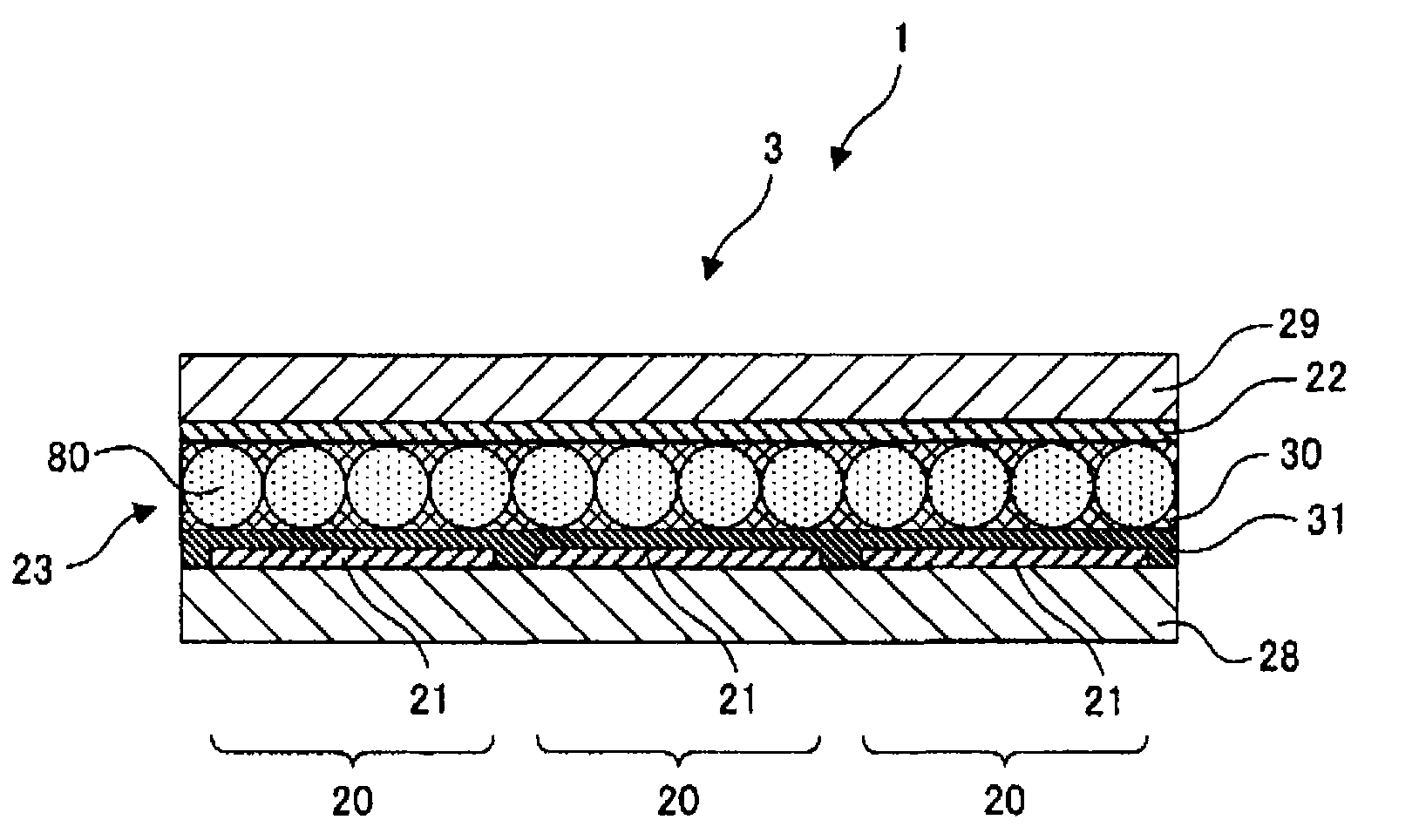
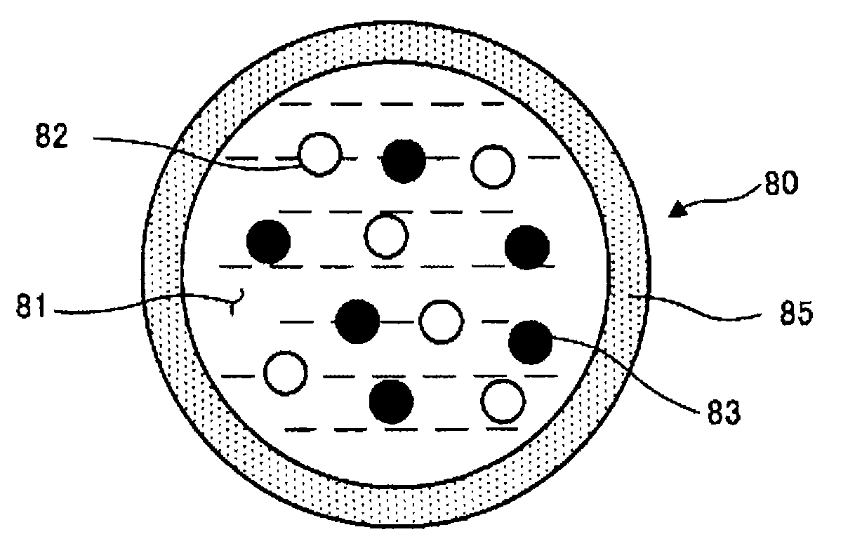
Electrophoretic display device and electronic apparatus
An electrophoretic display and electrophoresis technology, applied in static indicators, nonlinear optics, instruments, etc., can solve problems such as electrostatic potential difference and electrostatic damage, and achieve the effect of preventing electrostatic damage
- Summary
- Abstract
- Description
- Claims
- Application Information
AI Technical Summary
Problems solved by technology
Method used
Image

Examples
no. 1 Embodiment approach
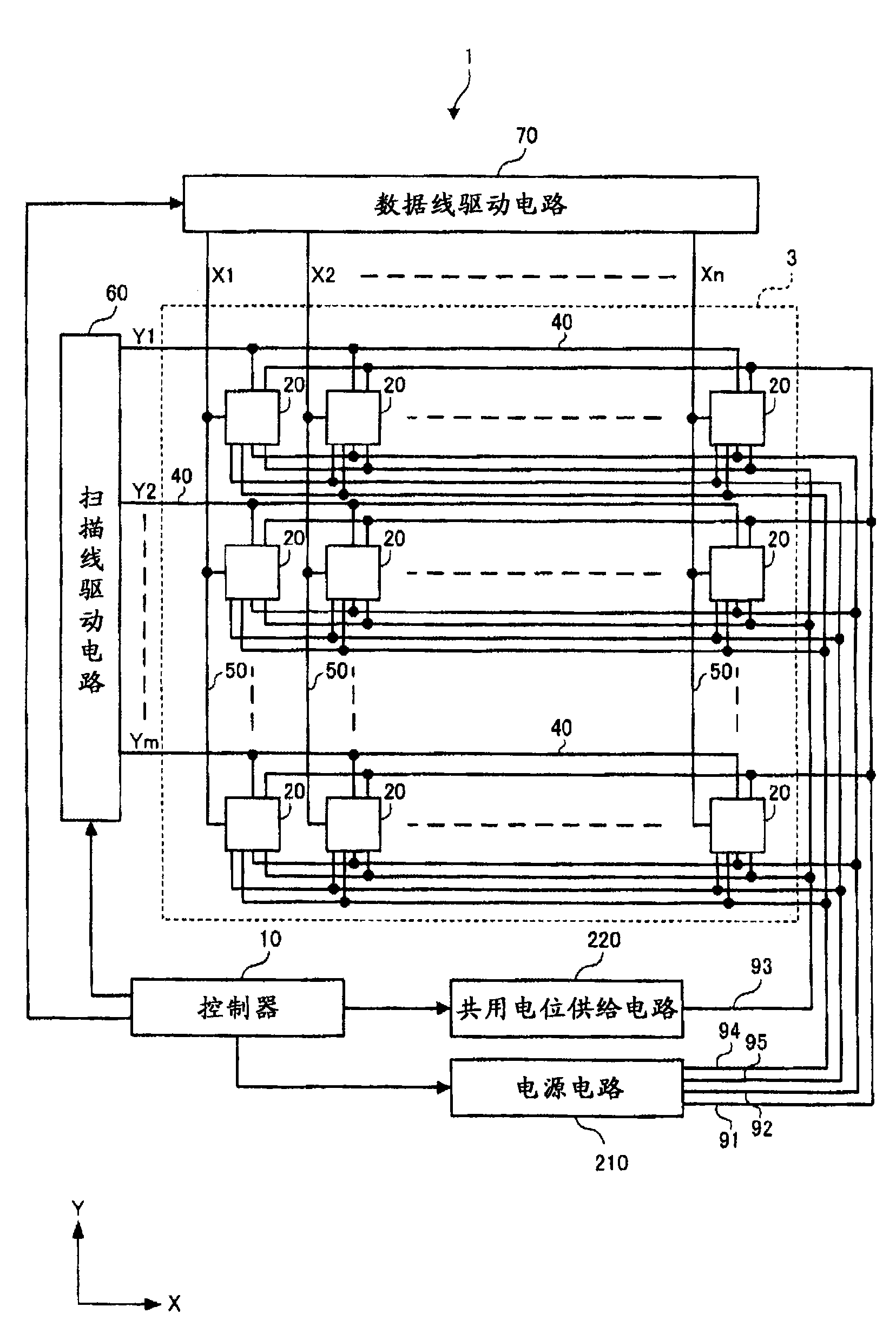
[0056] For the electrophoretic display device in the first embodiment, refer to Figure 1 ~ Figure 4 Be explained.
[0057] First, regarding the overall configuration of the electrophoretic display device in this embodiment, refer to figure 1 Be explained.
[0058] figure 1 , is a block diagram showing the overall configuration of the electrophoretic display device in the first embodiment.
[0059] exist figure 1 Among them, the electrophoretic display device 1 in the first embodiment includes a display unit 3 , a controller 10 , a scanning line driving circuit 60 , a data line driving circuit 70 , a power supply circuit 210 , and a common potential supply circuit 220 .
[0060] In the display unit 3 , pixels 20 of m rows×n columns are arranged in a matrix (two-dimensional plane). In addition, in the display unit 3, m scanning lines 40 (ie, scanning lines Y1, Y2, . . . , Ym) and n data lines 50 (ie, data lines X1, X2, . set crosswise. Specifically, m scanning lines 40 e...
no. 2 Embodiment approach
[0119] Next, regarding the electrophoretic display device in the second embodiment, refer to Figure 8 Be explained. In addition, the second embodiment differs from the above-mentioned first embodiment in that the circuit configuration in each pixel is different, and the other configurations are basically the same. Therefore, in the second embodiment, parts different from those in the first embodiment will be described in detail, and descriptions of other configurations will be appropriately omitted.
[0120] Figure 8 , is an equivalent circuit diagram showing the electrical configuration of a pixel in the electrophoretic display device according to the second embodiment. Also, in Figure 8 in, in and shown in figure 2 Components that are the same as those in the first embodiment are denoted by the same reference numerals.
[0121] exist Figure 8 Among them, the pixel 20 in the electrophoretic display device of the second embodiment includes a pixel switching transist...
no. 3 Embodiment approach
[0128] Next, regarding the electrophoretic display device in the third embodiment, refer to Figure 9 Be explained. In addition, the third embodiment differs from the first and second embodiments described above in that the circuit configuration in each pixel is different, but the other configurations are basically the same. Therefore, in the third embodiment, parts different from those of the first and second embodiments will be described in detail, and descriptions of other configurations will be appropriately omitted.
[0129] Figure 9 , is an equivalent circuit diagram showing the electrical configuration of a pixel in the electrophoretic display device of the third embodiment. Also, in Figure 9 in, in and shown in figure 2 Components that are the same as those in the first embodiment are denoted by the same reference numerals.
[0130] exist Figure 9 Among them, the pixel 20 in the electrophoretic display device of the third embodiment includes a pixel switching t...
PUM
 Abstract
Description
Claims
Application Information
 - R&D Engineer
- R&D Manager
- IP Professional
- Industry Leading Data Capabilities
- Powerful AI technology
- Patent DNA Extraction
Browse by: Latest US Patents, China's latest patents, Technical Efficacy Thesaurus, Application Domain, Technology Topic, Popular Technical Reports.
© 2024 PatSnap. All rights reserved.Legal|Privacy policy|Modern Slavery Act Transparency Statement|Sitemap|About US| Contact US: help@patsnap.com