Circuit board with conductive structure

A heat-conducting structure and circuit board technology, which can be used in circuits, multi-layer circuit manufacturing, printed circuits connected with non-printed electrical components, etc.

Active Publication Date: 2009-12-02
UNIMICRON TECH CORP
View PDF0 Cites 16 Cited by
  • Summary
  • Abstract
  • Description
  • Claims
  • Application Information

AI Technical Summary

Problems solved by technology

[0009] Although the second semiconductor chip 17" is stacked on the active surface 17a' of the first semiconductor chip 17' with the non-active surface 17b", the non-active surface 17b' of the first semiconductor chip 17' is still connected to In the carrier board 100 that cannot conduct heat and dissipate heat, the heat energy of the stacked semiconductor elements cannot be dissipated

Method used


Image

  • Circuit board with conductive structure
  • Circuit board with conductive structure
  • Circuit board with conductive structure

Examples


no. 1 example

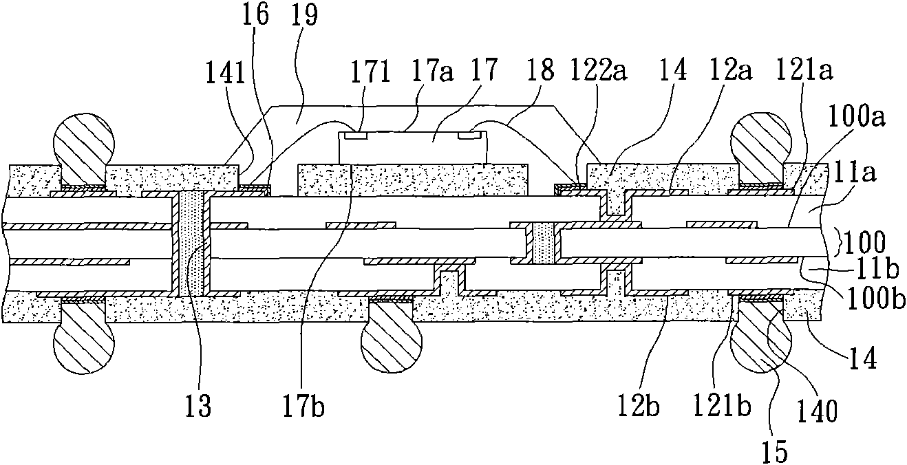
[0055] see Figure 3A to Figure 3F As shown in FIG. 2 , it is a schematic cross-sectional view illustrating the manufacturing method of the circuit board with the heat conduction structure according to the first embodiment of the present invention.

[0056] Such as Figure 3A and Figure 3A' As shown, at first, a carrier board is provided, and the carrier board is an insulating board or a circuit board 20 with lines 201. The surface 20a and the second surface 20b, and at least one through hole 200 penetrating through the first surface 20a and the second surface 20b, in the through hole 200 is formed a non-full plating metal conduction that is not electrically connected with the circuit 201 The first heat conduction structure 21a of the through hole (such as Figure 3A shown), or the first heat conduction structure 21a' that is fully plated with metal via holes (such as Figure 3A' shown), the first heat conduction structure 21a, 21a' is composed of the heat conduction hole...

no. 2 example

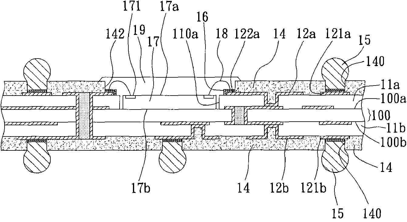
[0065] see Figure 4A and Figure 4B , is another embodiment of the present invention, wherein the Figure 4A What is shown is different from the previous embodiment in that the first and second heat conducting surfaces further include a metal layer, and the Figure 4B Shown with Figure 4A The difference is that the second heat conduction structure is a solid heat conduction blind hole.

[0066] Such as Figure 4A As shown, a metal layer 202 is formed on the surface of the circuit 201 on the first surface 20a and the second surface 20b of the circuit board 20, and covers the first and second heat conducting surfaces 211a, 212a of the first heat conducting structure 21a, so that the For example, the first and second heat conduction surfaces 211a, 212a at both ends of the heat conduction hole 210a of the non-full plated metal via hole are covered by the metal layer 202, so as to increase the contact area between the first heat conduction structure 21a and the semiconductor ...

no. 3 example

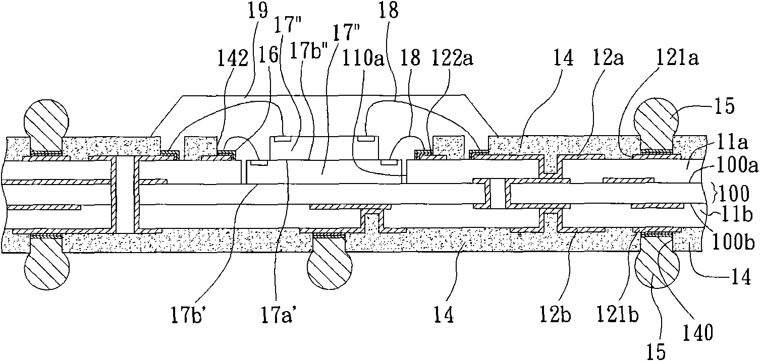
[0069] see Figure 5A to Figure 5C , is another embodiment of the present invention, the difference from the previous embodiment is that the first heat conduction structure is a solid heat conduction blind hole or a hollow heat conduction blind hole, and the second heat conduction structure is also a solid heat conduction blind hole or a hollow Thermally conductive blind vias.

[0070] Such as Figure 5AAs shown, the heat conduction hole 210a" in the circuit board 20 is a hollow heat conduction blind hole, and the second heat conduction structure 21b is also a hollow heat conduction blind hole, so that the heat conduction hole 210a" and the second heat conduction structure 21b are of the same type structure to simplify the manufacturing process.

[0071] Such as Figure 5B As shown, the heat conduction hole 210a" in the circuit board 20 is a hollow heat conduction blind hole, and the second heat conduction structure 21b' is a solid heat conduction blind hole, so that the he...


PUM


Abstract

The invention relates to a circuit board with a conductive structure, comprising a bearing board, a first conductive structure, a first dielectric layer, a second dielectric layer and a second conductive structure. The bearing board is provided with a first surface, a second surface and at least one through hole, and the first surface and the second surface are opposite; the first conductive structure comprises a conductive hole in the through hole, a first conductive surface arranged on the first surface of the bearing board and a second conductive surface arranged on the second surface; the first dielectric layer is arranged on the first surface of the bearing board and provided with a first opening so as to expose the first conductive surface; the second dielectric layer is arranged on the second surface of the bearing board and provided with at least one second opening so as to expose part of the second conductive surface; and the second conductive structure is arranged in the second opening and connected with the second conductive surface. The circuit board with the conductive structures also comprises a semiconductor element and a radiation element, wherein the passive surface of the semiconductor element is connected with the first conductive surface, and the radiation element is formed on the exposed surface of the second conductive structure so that heat can be radiated from the first conductive structure, the second conductive structure and the semiconductor element, and the semiconductor element and the circuit board can be protected against damage.

Description

technical field [0001] The invention relates to a circuit board structure, in particular to a circuit board with a heat conduction structure. Background technique [0002] With the evolution of semiconductor packaging technology, semiconductor devices (Semiconductor device) have developed different packaging types, among which ball grid array (BGA) is an advanced semiconductor packaging technology, which is characterized by the use of a package The substrate is used to carry and place the semiconductor chip, and a plurality of solder balls (Solderball) arranged in a grid array are formed on the back of the packaging substrate, so as to have more input / output connection terminals (I / Oconnection) in the same unit area to meet Highly integrated (Integration) semiconductor chips are required, and are electrically connected to external electronic devices through the solder balls. [0003] With the vigorous development of the electronic industry, electronic products are gradually...

Claims


Application Information

Patent Timeline
Patent Type & Authority Applications(China)
IPC IPC(8): H05K1/02H05K1/18H05K3/46H01L23/12H01L23/36H01L23/498H01L25/00
CPCH01L2224/48227H01L2924/0002H01L2224/48228H01L2224/48091H01L2924/15311H01L2924/15153H01L2224/32145H01L2924/00014
Inventor 周保宏朱志亮王维骏
Owner UNIMICRON TECH CORP
Why Eureka
Try Eureka