
Method and arrangement for manufacturing optical products with complex three-dimensional forms

A three-dimensional shape, complex technology, applied in the direction of semiconductor/solid-state device manufacturing, electrical components, circuits, etc., can solve problems such as unsolved, achieve the effect of easy construction and reduced duration

Active Publication Date: 2009-12-02
MODILIS HLDG LLC
View PDF0 Cites 7 Cited by
  • Summary
  • Abstract
  • Description
  • Claims
  • Application Information

AI Technical Summary

Problems solved by technology

[0011]While there are various existing methods for fabricating different microstructures on support surfaces, at least some of the aforementioned problems have not yet been addressed for high-precision micro-optical products. solve

Method used


Image

  • Method and arrangement for manufacturing optical products with complex three-dimensional forms
  • Method and arrangement for manufacturing optical products with complex three-dimensional forms
  • Method and arrangement for manufacturing optical products with complex three-dimensional forms

Examples


Embodiment Construction

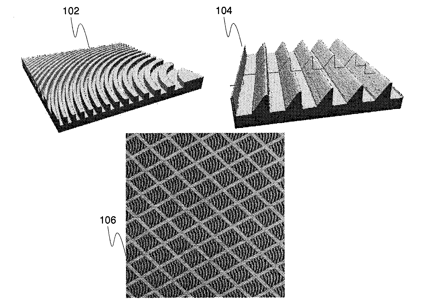
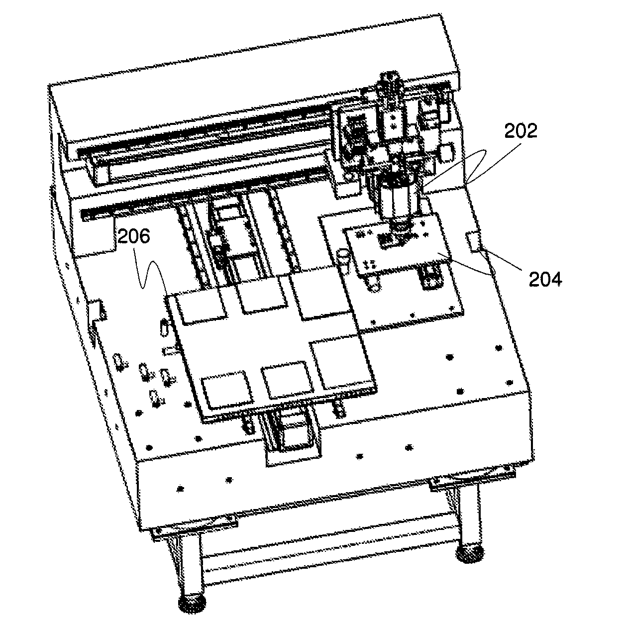
[0055] The advanced step embossing method according to the present invention typically utilizes multiple different embossing tools to produce variable micro-optical (eg DO) patterns with eg binary and / or blazed grating profiles. This profile is in the form of a surface relief pattern on the substrate. The substrate here is the material on which the micro-optical pattern is actually formed, and the substrate itself may be placed on top of a different carrier medium, eg as an uppermost layer. The imprint tool can be manufactured by high-precision micromachining or photolithography according to the required micro-optical structure. In addition, a novel imprint tool manufacturing method will be proposed hereinafter. Micromachining is more suitable for inclined structures such as 45° blazed gratings than photolithographic methods, however, photolithography is feasible for eg binary grooves. In microfabrication, generally, it is advantageous to focus on high-quality structures tha...


PUM

PropertyMeasurementUnit
wavelengthaaaaaaaaaa
refractive indexaaaaaaaaaa

Abstract

A method and an arrangement for manufacturing microoptic surface design with complex, variable three-dimensional forms. The method comprises obtaining (302) a step embossing, step imprinting, a chip bonding or a corresponding device capable of patterning the surface of a target substrate, obtaining the target substrate (304) whereto the micro-optic structures shall be patterned, obtaining a plurality of different stamping tools (306) operable with said device, each stamping tool comprising one or more surface relief forms defining one or more micro-optic structures, selecting (310) a stampingtool from said plurality of stamping tools by said device, embossing (312) the target substrate with said selected stamping tool as controlled by said device, wherein said selected stamping tool is optionally heated or assisted by UV (Ultraviolet) source so as to form and / or cure the target substrate during or after the embossing, and repeating (314) said selecting and embossing steps until the micro-optic surface design has been completed on the substrate. A related computer software product for control purposes is also disclosed.

Description

technical field [0001] In general, the present invention relates to optics and optoelectronics. In particular, the invention relates to methods of fabricating optical microstructures. Background technique [0002] There is an increasing need to improve light management and luminous efficiency in many lighting applications. This premise applies in particular to LED (Light Emitting Diode) lighting. To achieve the desired lighting performance, efficient optics with point light sources such as LEDs need to be used. Solutions utilizing diffractive optics or other complex micro-optical structures offer a host of new possibilities for advanced illumination including dimensional benefit and cost-effective integration. [0003] Typically, the fabrication of diffractive (DO) or other micro-optical structures is done by photolithographic processes such as mask lithography, direct laser beam or electron beam writing. These methods have certain disadvantages which greatly limit the f...

Claims


Application Information

Patent Timeline
Patent Type & Authority Applications(China)
IPC IPC(8): B29C59/00B29C59/02H01L21/68
CPCB29C59/02B29C59/00H01L21/68B29C67/00
Inventor 卡里·林科
Owner MODILIS HLDG LLC
Learn More