Wafer level fan-out chip packaging method

A chip packaging, wafer-level technology, applied in the field of wafer-level fan-out chip packaging, can solve the problem of low packaging cost, achieve the effect of reducing packaging cost and solving chip displacement

Active Publication Date: 2009-12-16
JIANGYIN CHANGDIAN ADVANCED PACKAGING CO LTD
View PDF0 Cites 41 Cited by
  • Summary
  • Abstract
  • Description
  • Claims
  • Application Information

AI Technical Summary

Problems solved by technology

[0009] The purpose of the present invention is to overcome the above disadvantages, and provide a wafer-level fan-out chip packaging method and packaging method with low packaging cost, tape carrier function, and a good solution to the problem of chip displacement in the process

Method used


Image

  • Wafer level fan-out chip packaging method
  • Wafer level fan-out chip packaging method
  • Wafer level fan-out chip packaging method

Examples


Embodiment Construction

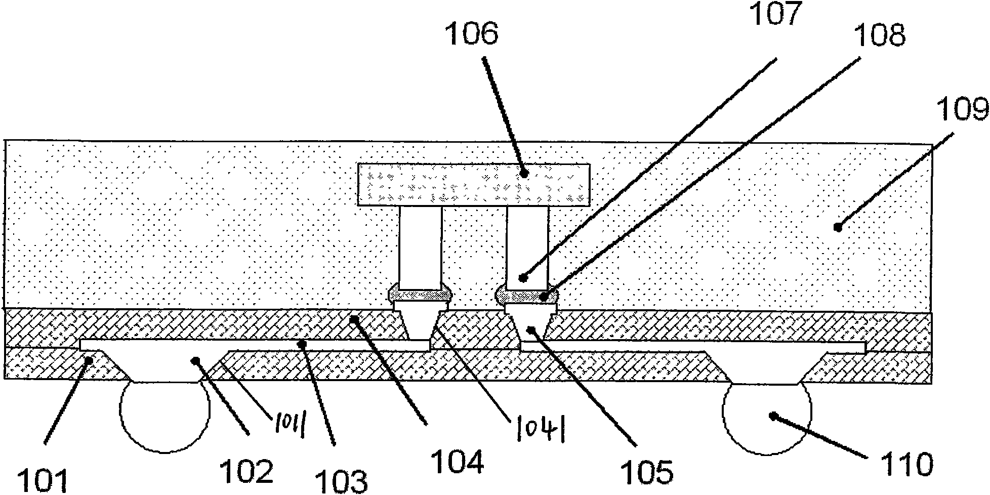
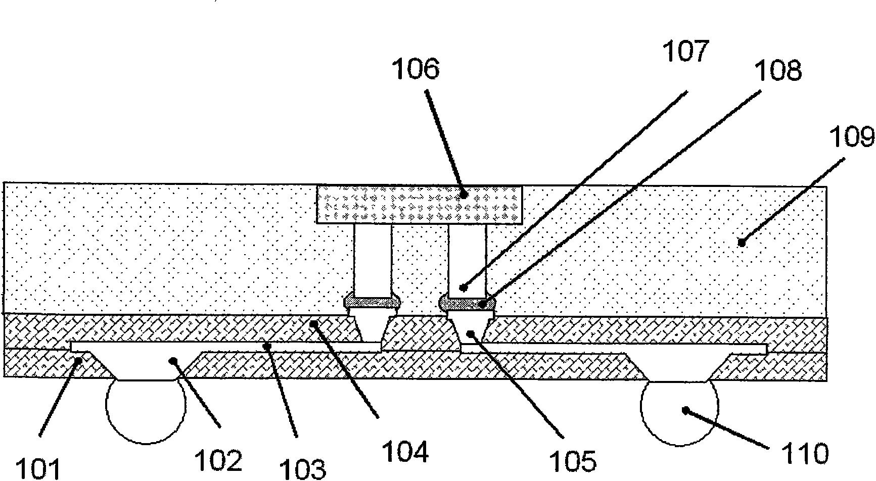
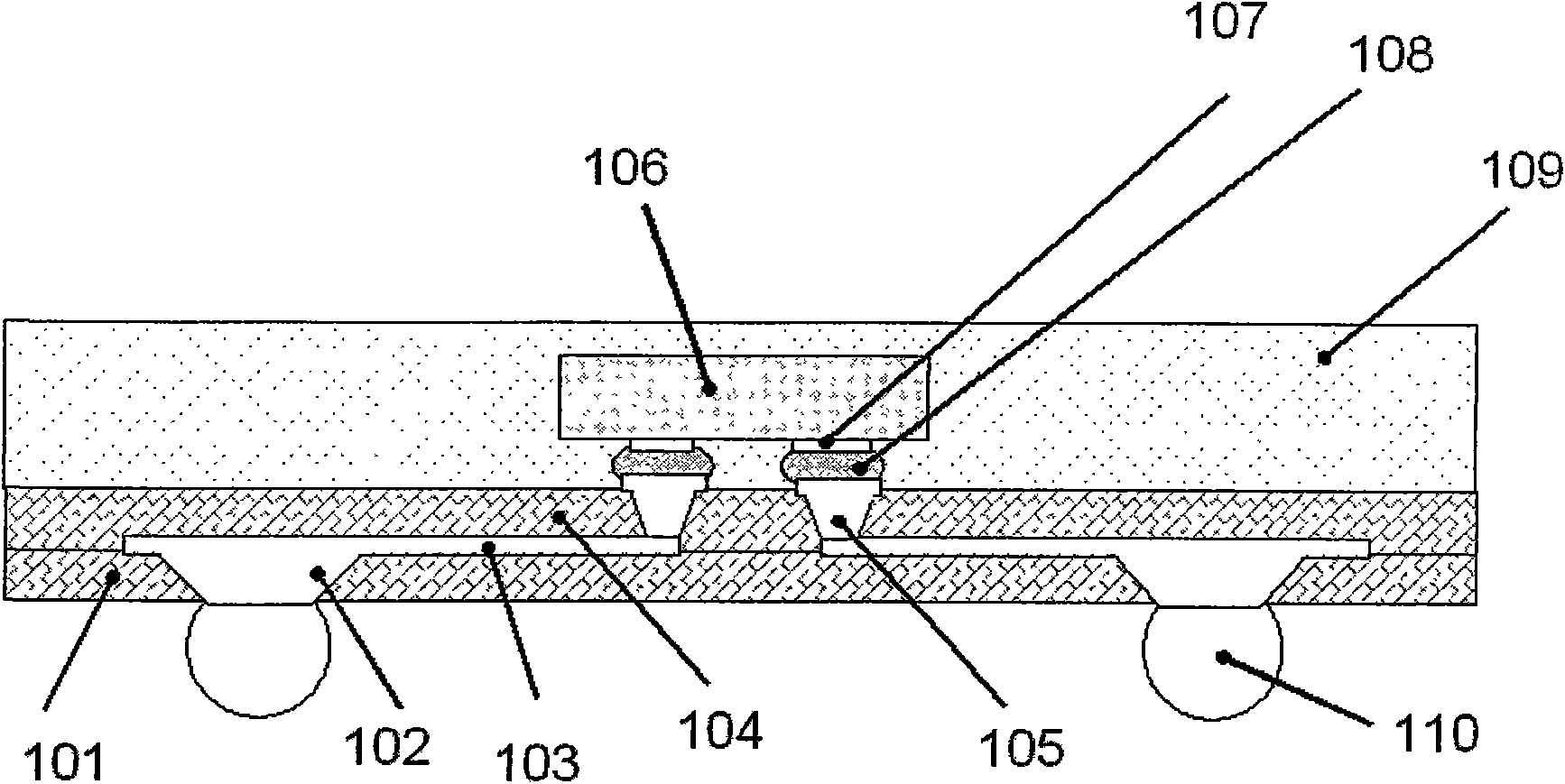
[0030] see figure 1 , the wafer-level fan-out (Fanout) chip packaging structure of the present invention includes a thin-film dielectric layer I 101, and a photolithographic pattern opening I 1011 is formed on the thin-film dielectric layer I 101, and the pattern opening I 1011 and the thin-film dielectric layer The surface of I 101 is provided with a metal electrode 102 connected to the substrate end and a redistribution metal trace 103, and the surface of the metal electrode 102 connected to the substrate end, the redistribution metal trace 103 surface, and the surface of the thin film dielectric layer I 101 are covered with Thin-film dielectric layer II104, on which a photolithographic pattern opening II 1041 is formed, and a metal electrode 105 connected to the chip end is arranged on the photolithographic pattern opening II 1041, which will have an IC chip 106, The chip of metal post / metal bump 107 and solder 108 is flip-chip mounted on the metal electrode 105 connected t...


PUM


Abstract

The invention relates to a wafer level fan-out chip packaging method, comprising the following technological processes: a stripping foil and a film dielectric layer I are sequentially covered on the surface of the wafer of a carrier, a photoetching pattern opening I is formed on the film dielectric layer I; a metal electrode and a re-wiring metal routing wire which are connected with a base plate end are arranged on the photoetching pattern opening and the surface thereof, a film dielectric layer II is covered on the surface of the metal electrode, the surface of the re-wiring metal routing wire, and the surface of the film dielectric layer I which are connected with the base plate end, and a photoetching pattern opening II is formed on the film dielectric layer II; a metal electrode connected with a chip end is arranged on the photoetching pattern opening II, after a chip is arranged on the metal electrode connected with the chip end in an inverting way, the injection molding of packaging material and solidification are carried out, so as to form a packaging body with plastic-packaging material; the wafer of the carrier and the stripping foil are separated from the packaging body with plastic-packaging material, so as to form a plastic-packaging wafer; a welding sphere back returns to form a welding ball salient point; cutting is carried out by uniwafers for forming the final structure of the fan-out chip. The method has low cost and a carrying function, and can well solve the problem that the chip is shifted in the technological process.

Description

(1) Technical field [0001] The invention relates to a chip packaging structure and a packaging method thereof. It belongs to the technical field of semiconductor chip packaging. (2) Background technology [0002] In the current semiconductor industry, electronic packaging has become an important aspect of industry development. With the development of packaging technology for decades, the traditional peripheral wiring low-pin-count packaging form is increasingly unable to meet the current high-density and small-size packaging requirements. Perimeter routing to area array routing provides a complete solution. Its advantages are: [0003] The number of pins per unit chip area has increased. [0004] Compared with the traditional wire bonding structure, the ball grid array structure shortens the distance between the chip circuit and the substrate, increases the transmission speed of electrical signals, and improves the chip function. [0005] Due to the limitations of the s...

Claims


Application Information

Patent Timeline
Patent Type & Authority Applications(China)
IPC IPC(8): H01L21/50H01L21/60
CPCH01L2924/15311H01L2924/18161H01L2924/01078H01L2924/01079H01L2224/16H01L2224/16227H01L2224/81005
Inventor 张黎赖志明陈栋陈锦辉曹凯
Owner JIANGYIN CHANGDIAN ADVANCED PACKAGING CO LTD
Why Eureka
Try Eureka