Method for molding via hole of printed circuit board

A printed circuit board and molding method technology, applied in the direction of electrical connection formation of printed components, can solve the problems of poor adhesion of photosensitive resist film, unrealizable wiring structure, and restricted wiring density, etc., to achieve excellent electrical performance, Small area occupation, simple and feasible process

Active Publication Date: 2009-12-16
美龙翔微电子科技(深圳)有限公司
View PDF0 Cites 15 Cited by
  • Summary
  • Abstract
  • Description
  • Claims
  • Application Information

AI Technical Summary

Problems solved by technology

However, these traditional copper vias will have a great negative impact on the subsequent process flow. For example, in the transfer process of the circuit pattern after the hollow copper vias are formed, the unevenness of the substrate surface caused by the hollow vias will cause photosensitive resistance. Poor adhesion of the etch film can easily cause line defects
In addition, this kind of through hole will have a great influence on the wiring design, so that the hole layout on the racket is limited, so that special wiring structures such as stacked holes cannot be realized, thus restricting the improvement of wiring density

Method used


Image

  • Method for molding via hole of printed circuit board
  • Method for molding via hole of printed circuit board
  • Method for molding via hole of printed circuit board

Examples


Embodiment Construction

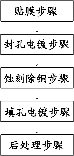
[0025] Such as Figure 3~Figure 10 As shown, the present invention provides a method for forming a via hole in a printed circuit board, which mainly includes the following steps:

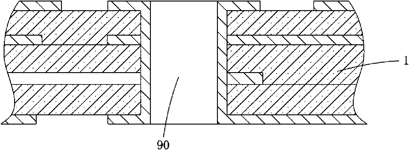
[0026] In the film sticking step, the double-sided copper-clad printed circuit board substrate (referred to as the substrate) that has been pre-drilled with via holes 10 by mechanical or laser means is pasted on the surface of the upper and lower copper layers 2 of the insulating dielectric layer 1 that need to be conductively connected. A photosensitive film 3 is attached, and a film opening 30 for limiting the electroplated copper area is formed on the photosensitive film 3 at a position corresponding to the via hole 10;

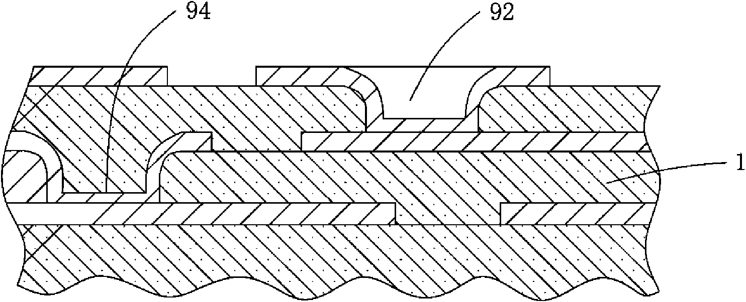
[0027] In the hole sealing electroplating step, on the first surface of the insulating dielectric layer 1, the film opening 30 formed in the film sticking step to limit the electroplating copper area is used, and the via hole 10 close to the first surface of the insulating diele...


PUM


Abstract

The invention relates to a method for molding a via hole of a printed circuit board, which comprises the steps of: film attachment, in which the surfaces of upper and lower surface copper layers of an insulating dielectric layer drilled with the via hole are attached with photosensitive films, and the positions, which correspond to the via hole, on the photosensitive films are provided with film openings; hole-sealing electroplating, in which an orifice end, which is near a first surface, of the via hole is closed through a copper electroplating process on the first surface of the insulating dielectric layer; hole-filling electroplating, in which the via hole is completely filled with copper, and the filled copper is connected with the surface copper layer of a second surface of the insulating dielectric layer, namely the connection of solid via holes between upper and lower adjacent line layer patterns is realized; and the post-treatment, in which the two surfaces of the insulating dielectric layer are subjected to subsequent treatment respectively, and a level conducting surface which is convenient for implementing subsequent pattern line production working procedures is obtained by removing the photosensitive films, removing the filled copper higher than the surface copper layers, and leveling the board surface. The method has the advantages of simple, convenient and feasible process, low cost, and small area occupation, and upper and lower corresponding line rackets of the hole are integrally preserved, are not damaged by the via hole and have good electrical properties.

Description

technical field [0001] The invention relates to a technology for preparing printed circuit boards, in particular to a method for forming via holes in printed circuit boards. Background technique [0002] With the development of integrated circuits, the requirements for integrated circuit packaging have also increased, and the requirements for printed circuit boards used in packaging are also developing towards higher wiring density, better electrical performance and thermal performance. In order to meet the above requirements, the development of high-reliability via hole technology is the key, which has a great impact on the density of wiring and the electrical and thermal performance after packaging. [0003] As we all know, there must be several via holes on the printed circuit board to connect the circuits on the upper and lower adjacent conductive surfaces of the insulating medium layer. Such as figure 1 As shown, one of the traditional via hole manufacturing methods i...

Claims


Application Information

Patent Timeline
Patent Type & Authority Applications(China)
IPC IPC(8): H05K3/42
Inventor 尤宁圻陈金福
Owner 美龙翔微电子科技(深圳)有限公司
Why Eureka
Try Eureka