Design and verification of 3d integrated circuits

An integrated circuit, 3D technology, used in CAD circuit design, computer-aided design, calculation, etc.

Active Publication Date: 2009-12-23
TAIWAN SEMICON MFG CO LTD
View PDF0 Cites 22 Cited by
  • Summary
  • Abstract
  • Description
  • Claims
  • Application Information

AI Technical Summary

Problems solved by technology

The interaction of the stacked dies raises larger design challenges that have not been addressed by designers, including developers of CAD tools

Method used


Image

  • Design and verification of 3d integrated circuits
  • Design and verification of 3d integrated circuits
  • Design and verification of 3d integrated circuits

Examples


Embodiment Construction

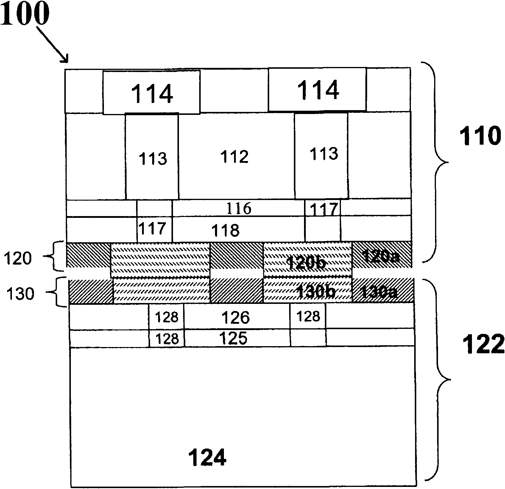
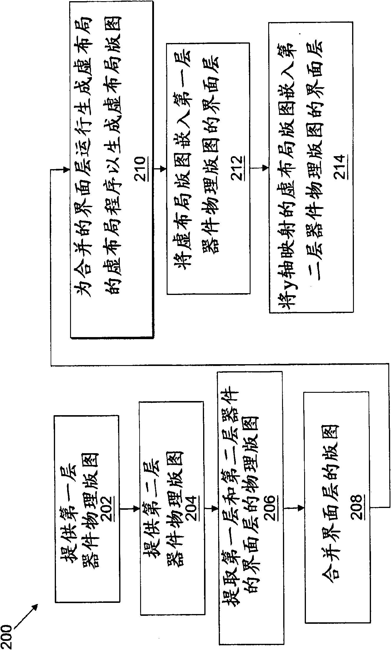
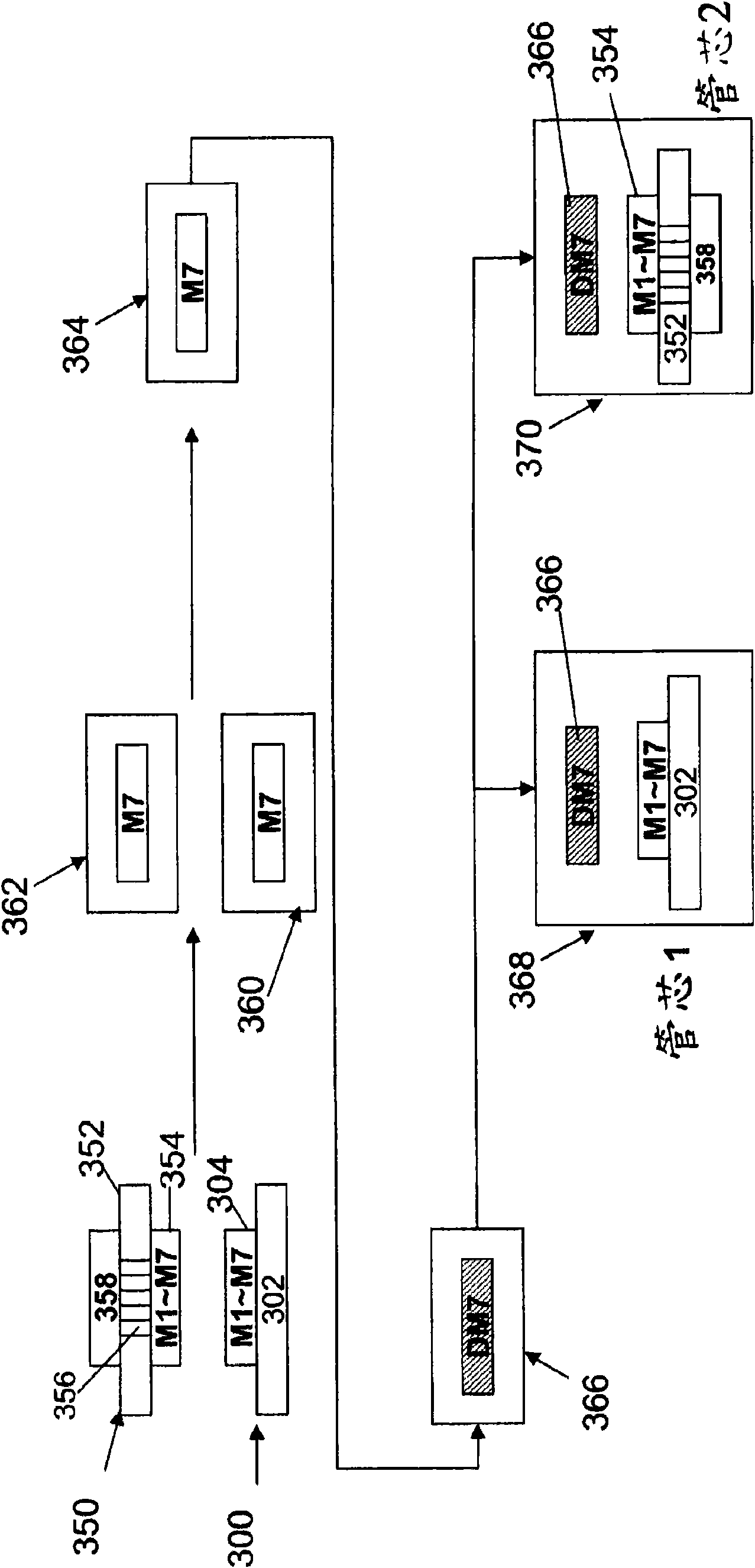
[0019] It will be appreciated that the specific embodiments provided herein are examples to teach the broader inventive concepts, and those skilled in the art can readily apply the teachings of the present invention to other methods and systems. Additionally, it is to be understood that the methods and systems discussed herein include some general structures and / or processes. Because these structures and processes are well known in the art, they will be discussed in general detail only. Reference numerals in the drawings may be repeated for convenience and illustration, and such repetition does not represent any necessary combination of features or steps in the drawings. Additionally, although methods for the design and verification of 3D ICs are described herein, those skilled in the art will recognize that other design processes may also benefit from the present disclosure. Verification methods including Layout Schematic Verification (LVS) and Design Rule Checking (DRC) for...


PUM


Abstract

A method of designing a 3D integrated circuit (3D IC) including providing a first layout corresponding to a first device of a 3D IC and a second layout corresponding to a second device of a 3D IC is provided. A verification, such as LVS or DRC, may be performed not only on each device separately, but may also be performed to ensure proper connectivity between devices. The verification may be performed on a single layout file (e.g., GDS II file) including the interface layer of the first and second die. Dummy feature pattern may be determined for the 3D IC using a layout including the interface layers of the first and second devices.

Description

technical field [0001] The present invention generally relates to the physical design and verification of three-dimensional (3D) integrated circuits. Background technique [0002] 3D integrated circuits (3D ICs) include semiconductor devices with two or more layers of active electronic components integrated (eg, vertically stacked and connected) to form an integrated circuit. Various forms of 3D IC technology are commonly developed, including die-die stacking, die-wafer stacking, and wafer-wafer stacking. In 3D IC technology, electronic components (such as integrated circuits) are disposed on two or more substrates and packaged to form a single integrated circuit. After being diced into individual dies or while in wafer form (possibly diced later), the electronic components are arranged and connected together. Vertical connections between electronic components, such as through the use of through-silicon vias (TSV) technology. The stacked die can then be packaged so that i...

Claims


Application Information

Patent Timeline
Patent Type & Authority Applications(China)
IPC IPC(8): G06F17/50
CPCG06F17/5068G06F30/39
Inventor 王中兴蔡志昇刘盈麟林凯筠
Owner TAIWAN SEMICON MFG CO LTD
Why Eureka
Try Eureka