Method of manufacturing semiconductur device

A manufacturing method and semiconductor technology, applied in semiconductor/solid-state device manufacturing, semiconductor devices, electric solid-state devices, etc., can solve problems such as uneven nitride film length, decreased uniformity of memory cells, and reduced reliability of semiconductor devices, etc., to achieve Effects of Preventing Changes in Characteristics

Inactive Publication Date: 2009-12-23
DONGBU HITEK CO LTD
View PDF1 Cites 10 Cited by
  • Summary
  • Abstract
  • Description
  • Claims
  • Application Information

AI Technical Summary

Problems solved by technology

[0012] When there is a difference between the length L1 of the first separation nitride film 120-1 and the length L2 of the second separation nitride film 120-2, the length of the separation charge trap nitride film of a memory cell such as a flash memory cell may vary. Uniformity, and the uniformity of the memory cell characteristics will decrease, therefore, the reliability of the semiconductor device will be reduced

Method used


Image

  • Method of manufacturing semiconductur device
  • Method of manufacturing semiconductur device
  • Method of manufacturing semiconductur device

Examples


Embodiment Construction

[0021] Hereinafter, reference will be made in detail to preferred embodiments of the present invention, examples of which are illustrated in the accompanying drawings.

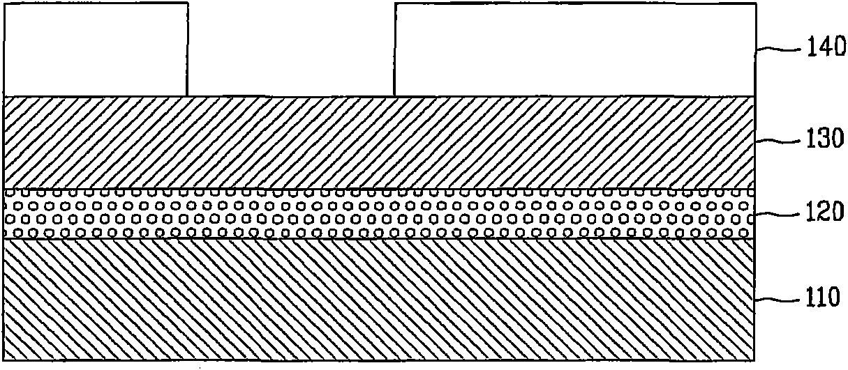
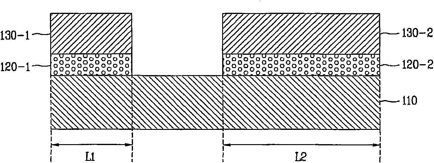
[0022] Figure 2A to Figure 2M is a longitudinal sectional view showing a method of manufacturing a semiconductor device according to an embodiment of the present invention.

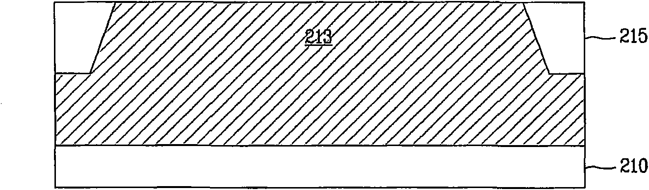
[0023] First, if Figure 2A As shown, an active region 213 and a device isolation region 215 are formed on a semiconductor substrate (eg, a p-type substrate) 210 . The active region 213 can be a p-type well or an n-type well.

[0024] For example, an epitaxial layer is grown on the semiconductor substrate 210, and then lightly doped with a p-type impurity, namely boron. Thereafter, a mask for forming the active region 213 is formed on the semiconductor substrate 210 using photolithography, and by using the mask (not shown) ions of an n-type impurity such as phosphorus implanted into the epitaxial layer to form an n-type well. In ord...


PUM


Abstract

Disclosed is a method of manufacturing a semiconductor device. The method includes forming an oxide-nitride-oxide (ONO) layer over a semiconductor substrate, and forming a recess over the semiconductor substrate by etching the ONO layer, forming a vertical structure pattern being higher than the ONO layer over the recess, sequentially forming a spacer oxide film and a first gate poly over the side wall of the vertical structure pattern, and forming a nitride film spacer at a partial region of the side wall of the first gate poly, removing the nitride film spacer, and forming a second gate poly in a spacer shape over the side wall of the first gate poly, and forming a first split gate and a second split gate, symmetrically divided from each other, by removing the vertical structure pattern. The invention can prevent the characteristic between the memory units based on the registration photoetching precision change in photolithography.

Description

[0001] This application claims priority from Korean Patent Application No. 10-2008-0058229 filed on Jun. 20, 2008, which is hereby incorporated by reference in its entirety. technical field [0002] The invention relates to a manufacturing method of a semiconductor device, in particular to a split gate type semiconductor memory device. Background technique [0003] Nonvolatile semiconductor memory devices are capable of electrically erasing and storing data, and retain data even when power is not supplied to the memory device, and thus are increasingly used in various fields including mobile communication systems and memory cards. [0004] Among these nonvolatile memory devices, a flash memory device is a memory device capable of executing a program for each cell and capable of erasing data for each block or sector. [0005] Since the flash memory device uses a conductive material such as doped polysilicon as a floating gate material, parasitic capacitance between adjacent g...

Claims


Application Information

Patent Timeline
Patent Type & Authority Applications(China)
IPC IPC(8): H01L21/8247H01L21/28H01L21/311
CPCH01L29/4234H01L29/792H01L21/28282H01L27/11568Y10S438/954H01L29/40117H10B43/30H01L21/28141H01L21/3213
Inventor 郑熙炖
Owner DONGBU HITEK CO LTD
Why Eureka
Try Eureka