Method, system and semiconductor processing equipment for reducing particle deposition in cavity

A semiconductor and chamber technology, applied in the field of microelectronics, can solve the problems affecting the process performance and service life of semiconductor processing equipment, corrosion of the inner wall of the vacuum lock chamber, etc., and achieve the effect of reducing deposition and avoiding damage

Active Publication Date: 2011-07-27
BEIJING NAURA MICROELECTRONICS EQUIP CO LTD
View PDF0 Cites 0 Cited by
  • Summary
  • Abstract
  • Description
  • Claims
  • Application Information

AI Technical Summary

Problems solved by technology

Since these process gas particles include HBr, Cl 2 Such corrosive gas particles, therefore, when attached to the inner wall of the vacuum lock chamber, will cause corrosion to t

Method used


Image

  • Method, system and semiconductor processing equipment for reducing particle deposition in cavity
  • Method, system and semiconductor processing equipment for reducing particle deposition in cavity
  • Method, system and semiconductor processing equipment for reducing particle deposition in cavity

Examples


Example Embodiment

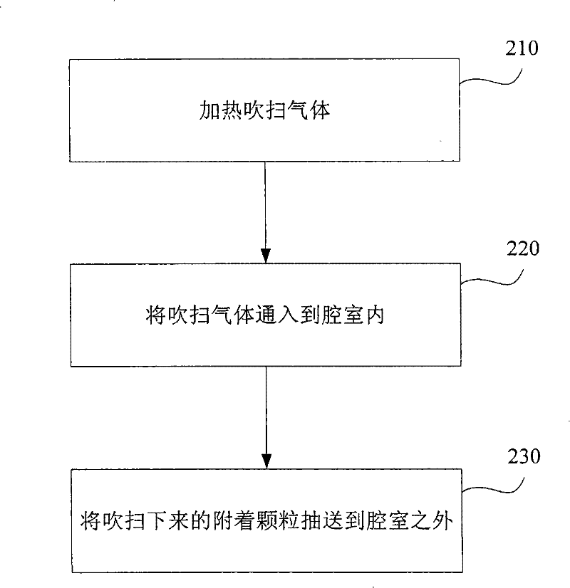
[0037]The core of the present invention is: introducing into the chamber a gas (such as N 2 etc.), and by means of the natural convection of the air in the chamber, the particles adhering to the inner wall of the chamber are swept off, so that the inner wall of the chamber is prevented from being attacked by the above-mentioned particle corrosion and the like.

[0038] In order to make those skilled in the art better understand the technical solutions of the present invention, the following steps are used to pass through the chamber, such as N 2 The method and system for reducing the deposition of particles in the chamber and the semiconductor processing equipment using the method and / or system provided by the present invention are described in detail.

[0039] In the method for reducing the deposition of particles in the chamber provided by the present invention, firstly, the N to enter the chamber is 2 Heating, and ensure that the temperature after entering the chamber is h...


PUM


Abstract

The invention discloses a method for reducing particle deposition in a cavity. The method comprises the following steps of: heating sweeping gas in a charging subsystem so as to make the temperature of the sweeping gas entering the cavity higher than the ambient temperature in the cavity; and introducing the heated sweeping gas into the cavity to sweep the attaching particles attached to the inner wall of the cavity by means of the natural convection between cold and hot gases so as to reduce or avoid the deposition of the attaching particles on the inner wall in the cavity. In addition, the invention also provides a system for reducing the particle deposition in the cavity and the semi-conductor processing equipment for using the method and/or system. The method, the system and the semiconductor processing equipment have the advantages of reducing the deposition of the particles in the cavity, correspondingly reducing or even avoiding the erosion of the particles in the cavity, and improving the service life of the cavity and the service life of the corresponding semiconductor equipment.

Description

technical field [0001] The present invention relates to the technical field of microelectronics, in particular, to a method and system for reducing particle deposition in a chamber, and semiconductor processing equipment using the method and / or system. Background technique [0002] With the rapid development of electronic technology, people have higher and higher requirements for the integration of integrated circuits, which requires companies that produce integrated circuits to continuously improve the processing / processing capabilities of semiconductor devices. Currently, plasma processing techniques such as plasma deposition techniques, plasma etching techniques, and the like are widely used in the processing / processing of semiconductor devices. These plasma processing technologies usually need to be realized by means of corresponding semiconductor processing equipment. [0003] see figure 1 , the existing semiconductor processing equipment generally includes a pumping ...

Claims


Application Information

Patent Timeline
IPC IPC(8): B08B5/02B08B13/00H01L21/00
Inventor 陈德高
Owner BEIJING NAURA MICROELECTRONICS EQUIP CO LTD
Why Eureka
Try Eureka