Protection sealing ring used for preventing stress caused by cutting die

A sealing ring and chip technology, used in electrical components, electrical solid devices, circuits, etc., can solve the problem of crack propagation without sufficient strength, and achieve the effect of reducing crack propagation

Active Publication Date: 2009-12-30
TAIWAN SEMICON MFG CO LTD
View PDF0 Cites 29 Cited by
  • Summary
  • Abstract
  • Description
  • Claims
  • Application Information

AI Technical Summary

Problems solved by technology

Second, continuous via bars typically have a width that is substantially less than the thickness of each overlying metal line, and thus do not have sufficient strength to prevent crack propagation during die sawing.
Third, cracks may propagate through the interface 22 between the passivation film 20 and the underlying layer into the circuit area

Method used


Image

  • Protection sealing ring used for preventing stress caused by cutting die
  • Protection sealing ring used for preventing stress caused by cutting die
  • Protection sealing ring used for preventing stress caused by cutting die

Examples


Embodiment Construction

[0016] The making and using of the embodiments are discussed in detail below. It should be appreciated, however, that the embodiments present many applicable inventive concepts that can be implemented in a wide variety of specific contexts. The specific embodiments discussed are merely illustrative of specific ways to make and use the invention, and do not limit the scope of the invention.

[0017] A seal ring structure with improved crack resistance and a method of forming the same are provided. Variations of this embodiment are also discussed. The same reference numerals are used to refer to the same elements throughout the various views and exemplary embodiments of the invention.

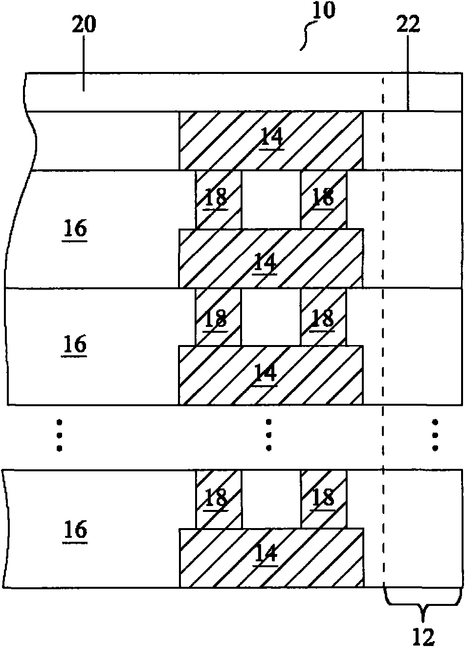
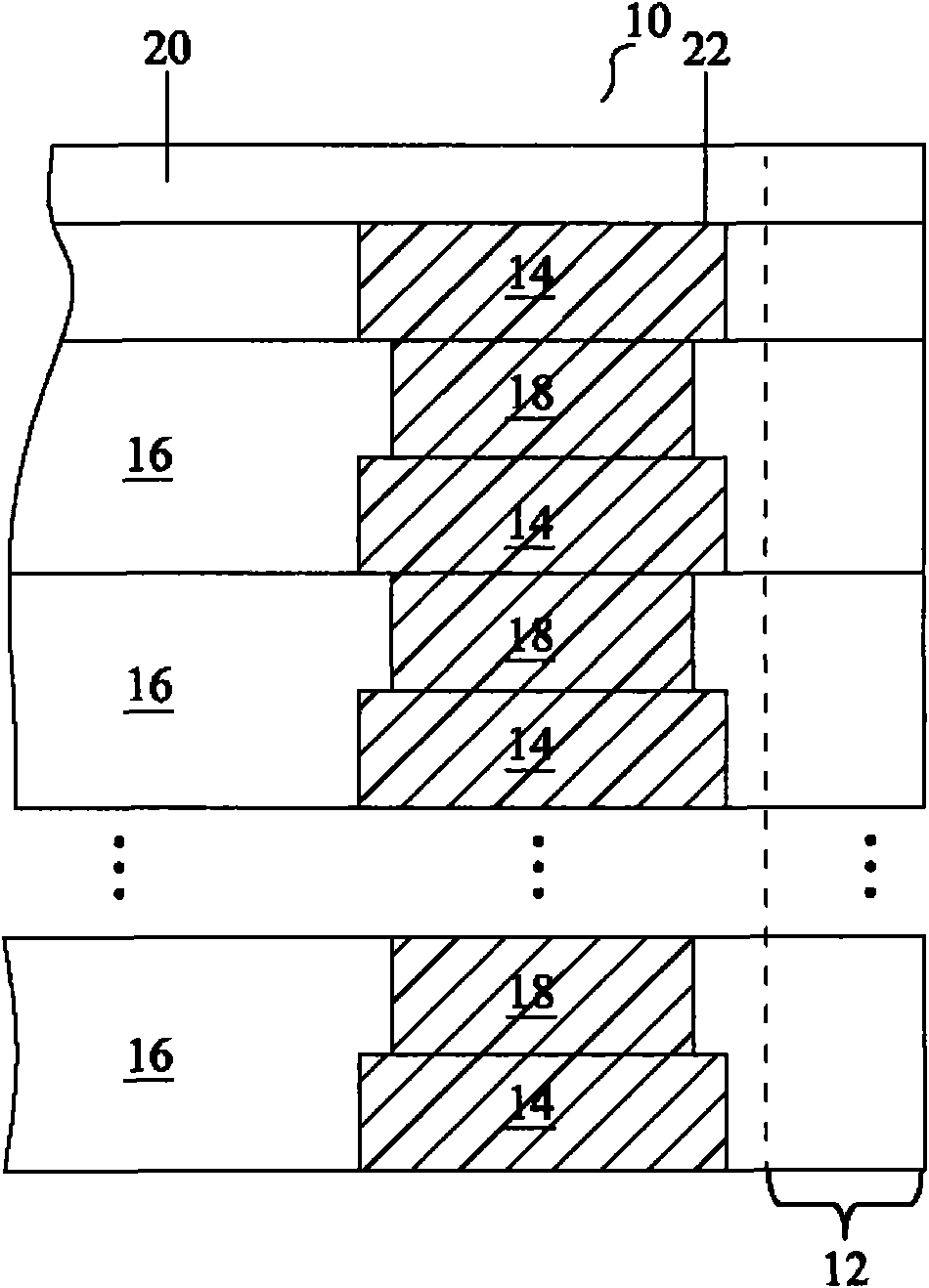
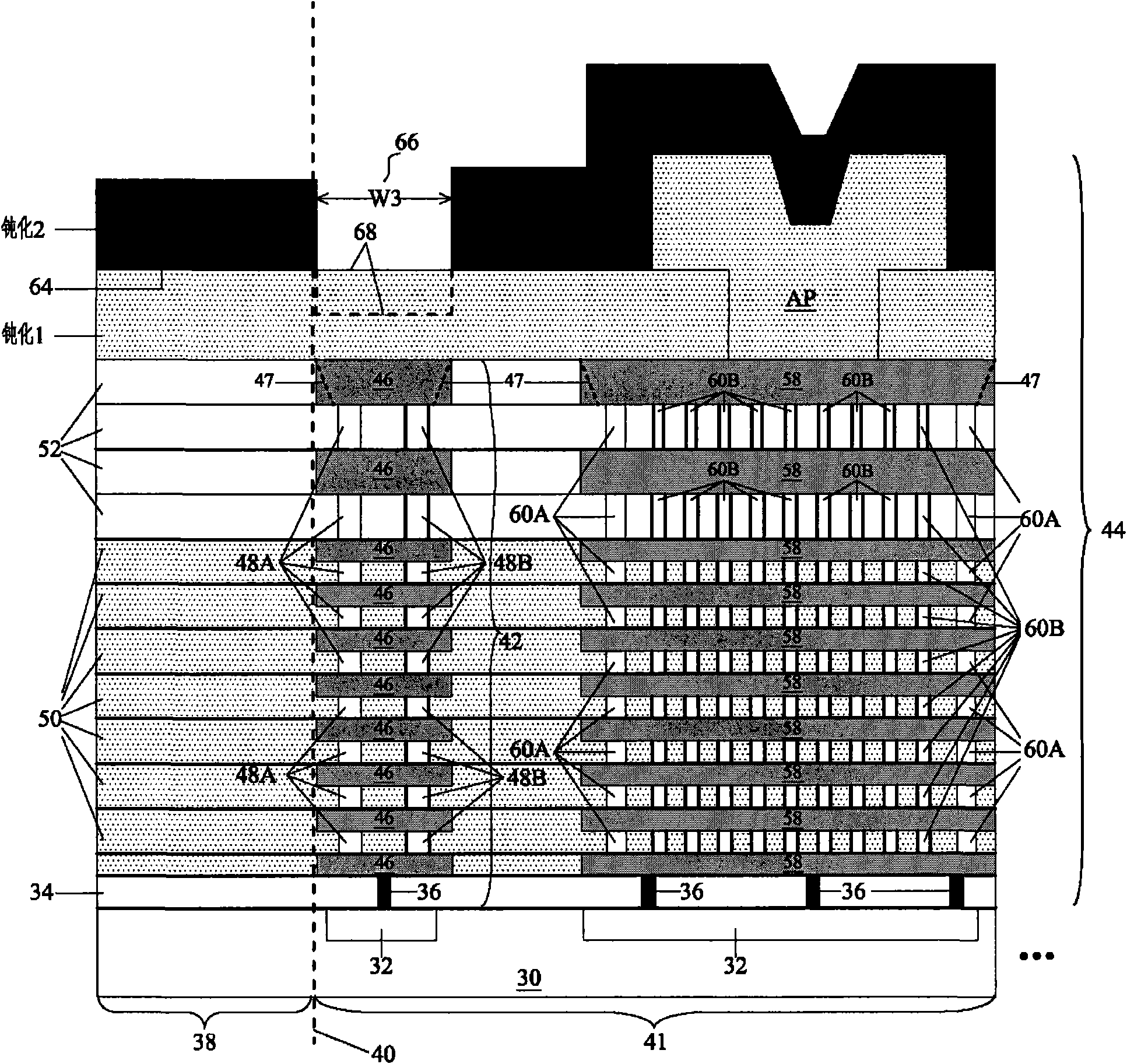
[0018] attached Figure 3A A first embodiment of the invention is shown. A portion of the semiconductor wafer includes a semiconductor substrate 30, which may be formed from silicon or other Group III, IV and / or V elements. The semiconductor substrate 30 may be lightly doped with p-type impu...


PUM


Abstract

The invention provides a semiconductor chip, comprising a semiconductor substrate; a plurality of low-k dielectric layers above the semiconductor substrate; a first passivation layer above a plurality of the low-k dielectric layers; and a second passivation layer above the first passivation layer. A first sealing ring is adjacent to an edge of the semiconductor chip, and the first sealing ring has an upper surface that is basically parallel and level with a bottom surface of the first passivation layer. The second sealing ring is adjacent to the first sealing ring and located at the inner side of the semiconductor chip. The second sealing ring comprises a bonding pad ring in the first passivation layer and the second passivation layer. A groove ring comprises at least a part that is directly formed above the first sealing ring, and extended downwards from a top surface of the second passivation layer at least to an interface between the first passivation layer and the second passivation layer.

Description

technical field [0001] The present invention relates to an integrated circuit, and more specifically, to a structure and a forming method of a sealing ring. Background technique [0002] Seal ring formation is an important part of the semiconductor back-end process. A seal ring is a stress protection structure surrounding an integrated circuit that protects internal circuitry within a semiconductor chip from damage caused by dicing a wafer into semiconductor chips. [0003] A typical seal ring is usually formed of interconnected metal lines and connecting vias. figure 1 is a schematic diagram of a portion of the seal ring 10 formed on the inner side of a scribe line (or called a scribe groove) 12 , which is sometimes also referred to as a dicing line 12 . Typically, there is a circuit area (not shown) on the left hand side of the drawing. [0004] Seal ring 10 includes interconnected metal elements formed from metal lines 14 and conductive vias 18 each formed in dielectri...

Claims


Application Information

Patent Timeline
Patent Type & Authority Applications(China)
IPC IPC(8): H01L23/00H01L23/58
CPCH01L23/564H01L23/585H01L23/562H01L21/78H01L2924/0002H01L2924/00
Inventor 郑心圃陈宪伟侯上勇蔡豪益吴念芳刘豫文
Owner TAIWAN SEMICON MFG CO LTD
Why Eureka
Try Eureka