Semiconductor chips with crack stop regions for reducing crack propagation from chip edges/corners

a technology of semiconductors and crack stops, applied in the field of semiconductor chips, can solve the problems of cracks likely to occur at chip edges/corners and propagate to the center of the chip, and achieve the effect of reducing crack propagation

Inactive Publication Date: 2010-06-08
GLOBALFOUNDRIES INC
View PDF9 Cites 1 Cited by
  • Summary
  • Abstract
  • Description
  • Claims
  • Application Information

AI Technical Summary

Benefits of technology

[0004]The present invention provides a structure (and method of forming the same), that reduce crack propagation from chip edges / corners to the center of the chip.

Problems solved by technology

In a conventional semiconductor chip, cracks are likely to occur at chip edges / corners and propagate to the center of the chip.

Method used


Image

  • Semiconductor chips with crack stop regions for reducing crack propagation from chip edges/corners
  • Semiconductor chips with crack stop regions for reducing crack propagation from chip edges/corners
  • Semiconductor chips with crack stop regions for reducing crack propagation from chip edges/corners

Examples


Embodiment Construction

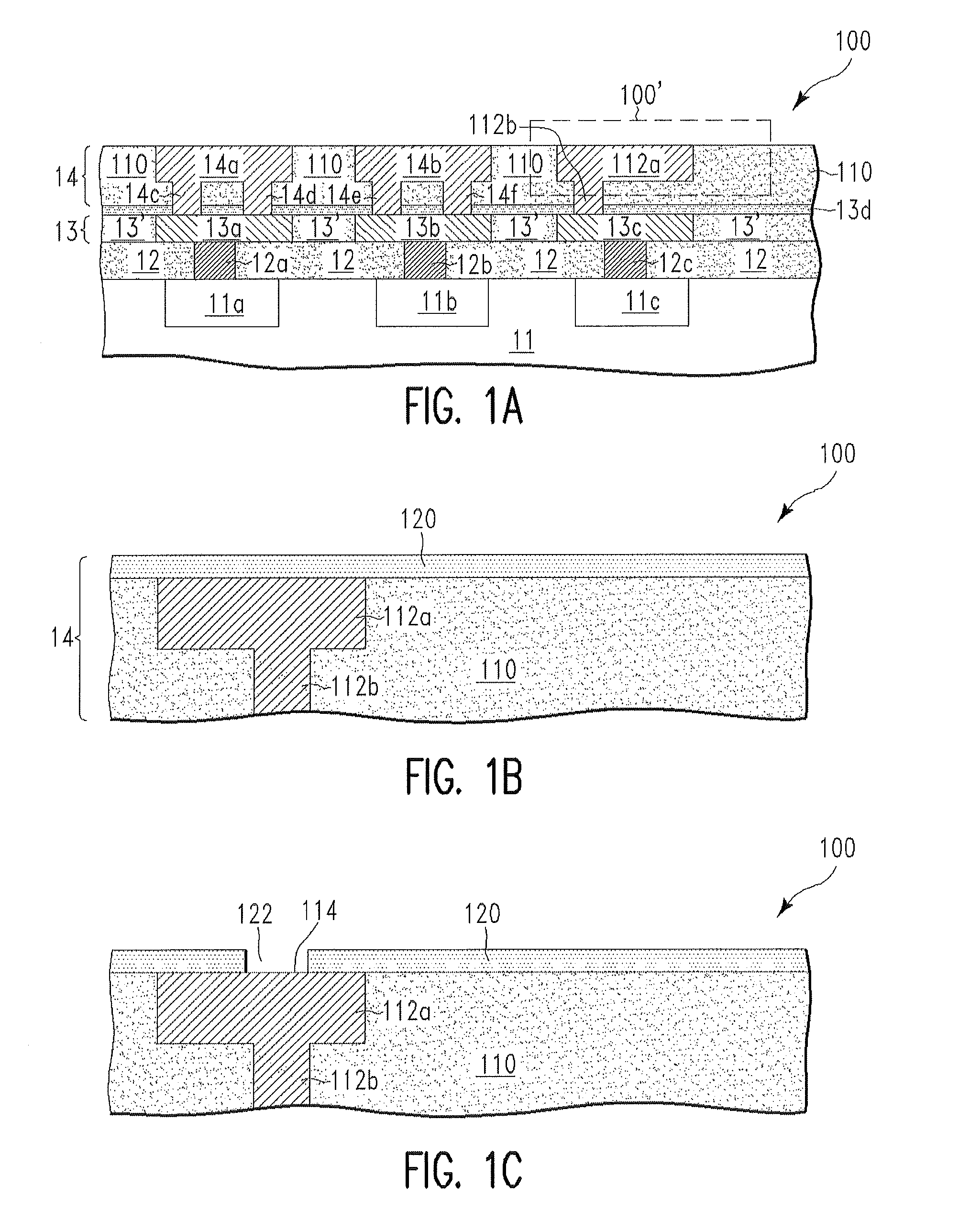
[0007]FIGS. 1A-1H (cross-section views) illustrate a fabrication process for forming a semiconductor chip 100, in accordance with embodiments of the present invention. More specifically, with reference to FIG. 1A, the fabrication process starts with the semiconductor structure 100. The semiconductor structure 100 comprises a semiconductor substrate 11 and transistors (only source / drain regions 11a, 11b, and 11c of the transistors are shown for simplicity) on the semiconductor substrate 11. The semiconductor structure 100 further comprises a BPSG (Boro-Phospho-Silicate Glass) layer 12 and contact regions 12a, 12b, and 12c in the BPSG layer 12. The contact regions 12a, 12b, and 12c can comprise tungsten and are electrically coupled to the source / drain regions 11a, 11b, and 11c, respectively.

[0008]The semiconductor structure 100 further comprises (i) an interconnect layer 13 including (a) a dielectric layer 13′, and (b) metal lines 13a, 13b, and 13c in the dielectric layer 13′, (ii) a ...


PUM


Abstract

Structures and a method for forming the same. The structure includes a semiconductor substrate, a transistor on the semiconductor substrate, and N interconnect layers on top of the semiconductor substrate, N being a positive integer. The transistor is electrically coupled to the N interconnect layers. The structure further includes a first dielectric layer on top of the N interconnect layers and P crack stop regions on top of the first dielectric layer, P being a positive integer. The structure further includes a second dielectric layer on top of the first dielectric layer. Each crack stop region of the P crack stop regions is completely surrounded by the first dielectric layer and the second dielectric layer. The structure further includes an underfill layer on top of the second dielectric layer. The second dielectric layer is sandwiched between the first dielectric layer and the underfill layer.

Description

FIELD OF THE INVENTION[0001]The present invention relates to semiconductor chips, and more specifically, to the semiconductor chips having crack stop regions that reduce crack propagation from chip edges / corners.BACKGROUND OF THE INVENTION[0002]In a conventional semiconductor chip, cracks are likely to occur at chip edges / corners and propagate to the center of the chip. Therefore, there is a need for a structure (and method of forming the same), that reduce crack propagation from chip edges / corners to the center of the chip.SUMMARY OF THE INVENTION[0003]The present invention provides a semiconductor chip, comprising (a) a semiconductor substrate; (b) a transistor on the semiconductor substrate; (c) N interconnect layers on top of the semiconductor substrate and the transistor, wherein N is a positive integer, and wherein the transistor is electrically coupled to the N interconnect layers; (d) a first dielectric layer on top of the N interconnect layers; (e) P crack stop regions on t...

Claims


Application Information

Patent Timeline
Patent Type & Authority Patents(United States)
IPC IPC(8): H01L23/492
CPCH01L21/563H01L23/3192H01L23/585H01L23/562H01L2924/01057H01L2224/73203
Inventor BROFMAN, PETER J.CASEY, JON ALFREDMELVILLE, IAN D.QUESTAD, DAVID L.SAUTER, WOLFGANGWASSICK, THOMAS ANTHONY
Owner GLOBALFOUNDRIES INC
Why Eureka
Try Eureka