Tunable multi-loop multi-system optical buffer based on N*N optical switch matrix

A technology of optical switch matrix and optical buffer, which is applied in the field of optical network communication, can solve the problems of many discrete components of optical buffer, uncompact structure, difficult performance control, etc., and achieve the effect of large dynamic adjustment range, simple structure and low cost

Inactive Publication Date: 2010-01-06
FUDAN UNIV
View PDF0 Cites 30 Cited by
  • Summary
  • Abstract
  • Description
  • Claims
  • Application Information

AI Technical Summary

Problems solved by technology

[0010] The present invention proposes a new type of multi-loop multi-ary system optical buffer based on N×N semiconductor active vertical coupler AVC (active vertical coupler) optical switch matrix. This scheme realizes a wide rang

Method used


Image

  • Tunable multi-loop multi-system optical buffer based on N*N optical switch matrix
  • Tunable multi-loop multi-system optical buffer based on N*N optical switch matrix
  • Tunable multi-loop multi-system optical buffer based on N*N optical switch matrix

Examples


Embodiment Construction

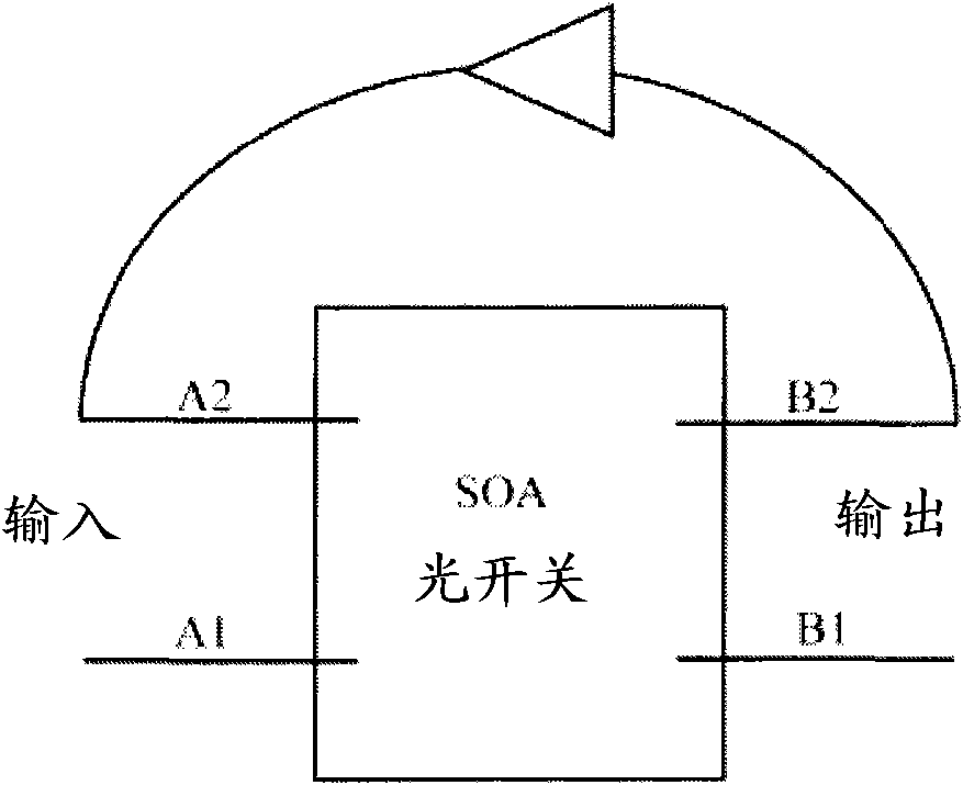
[0035] Such as Figure 4 What is shown is a 5×5 structure based on an active vertically coupled optical switch matrix. For a 5×5 OXS matrix, there are 25 optical switch units, and there are 5 input ports A1~A5 and 5 output ports D1 ~D5. Such as Figure 5 As shown, AB is the horizontal direction, CD is the vertical direction, the lower layer of the cross structure is a passive optical waveguide, and the upper layer is an active vertical coupler. The control principle of the optical switch control module to the optical switch unit is as follows: the signal light is input by A, when the optical switch control part does not inject DC light into the optical switch unit, the switch is in the off state, and the signal light will pass through the unit directly. Figure 5 As shown in part (a), when the optical switch control part injects DC light into the optical switch unit, the switch is in the trigger-on state, and the signal light will be reversed by 90 degrees. At this time, as ...


PUM


Abstract

The invention relates to the technical field of optical network communication, in particular to a tunable multi-loop multi-system optical buffer based on an N*N optical switch matrix, comprising an N*N optical switch matrix, an optical switch control module and N-1 optical delayers, wherein the delay time of the N-1 optical delayers is designed to be K times with each other, i.e. the delay time meets a K system relation; if rotation cycles of light in each loop are respective n1, n2, ..., n<N-1>, the total delay time of the buffer is T=n1d1+n2d2+...+n<N-1>d<N-1>, and the least delay time of the optical delayer can be designed by adjustable least precision according to the requirements. The adjusting speed of the optical buffer can reach nanosecond class high-speed response, the adjusting precision is high and stable, and the large dynamic adjusting range can be realized; and the optical buffer has simple structure, low cost and high reliability. The optical buffer capable of flexibly tuning in the large dynamic range has a practical meaning in optical packet switching, all-optical calculation, optical information processing and optical synchronous time slot alignment.

Description

technical field [0001] The invention relates to the technical field of optical network communication, and more specifically relates to a new optical buffer mechanism, that is, a tunable multi-loop multi-ary optical buffer based on an N*N optical switch matrix is ​​proposed. Background technique [0002] In the optical packet switching network, the optical buffering technology is the basic function of all all-optical routers, which is determined by the three main functional requirements of the router: First, due to the burst arrival of packets, when more than one packet When it arrives, some packets need to be buffered for queuing processing; secondly, in practice, it is also necessary to delay buffer the effective data part of the packet, so as to wait for the processing of the packet header to be completed; thirdly, the optical buffer for the data packet It is critical for clock synchronization and reorganization of newly formed tag heads. [0003] Theoretically, the buffe...

Claims


Application Information

Patent Timeline
IPC IPC(8): H04Q11/00H04B10/20
Inventor 迟楠张俊文
Owner FUDAN UNIV
Why Eureka
Try Eureka