Semiconductor process unit and focusing ring thereof
A technology of process equipment and focus ring, applied in semiconductor/solid-state device manufacturing, discharge tube, electrical components, etc., can solve problems such as affecting process quality, deposit warping or avalanche, large operating temperature difference, etc.
- Summary
- Abstract
- Description
- Claims
- Application Information
AI Technical Summary
Problems solved by technology
Method used
Image

Examples
Embodiment Construction
[0027] In order to make the above-mentioned objects, features and advantages of the present invention more comprehensible, preferred embodiments are specifically described below together with the attached drawings.
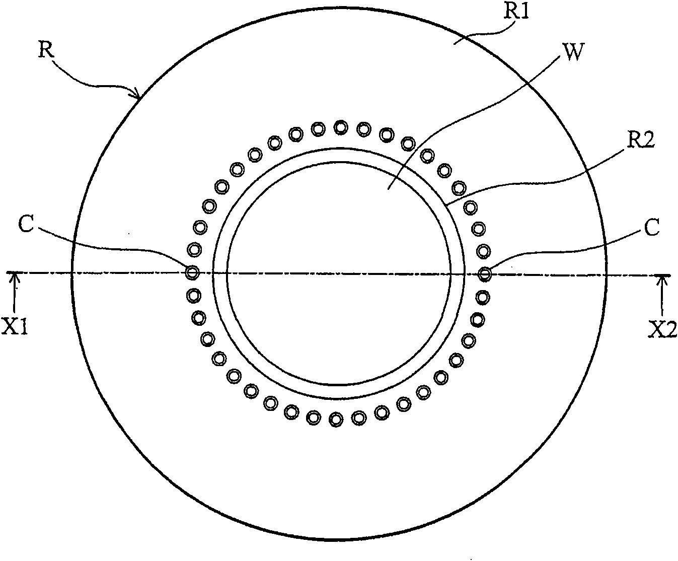
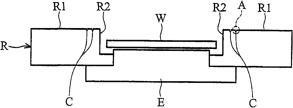
[0028] First, please also refer to figure 1 , figure 2 ,in figure 2 is along figure 1 Sectional view of X1-X2 in the middle.
[0029] Such as figure 2 As shown, the semiconductor process device according to an embodiment of the present invention mainly includes a circular focus ring R and an electrostatic chuck E (Electro-Static Chuck). The above-mentioned focus ring R and electrostatic chuck E are both arranged in a process reaction chamber, wherein A semiconductor wafer W is accommodated in a circular opening R2 in the center of the focus ring R, and an electrostatic chuck E is disposed below the focus ring R for fixing the semiconductor wafer W.
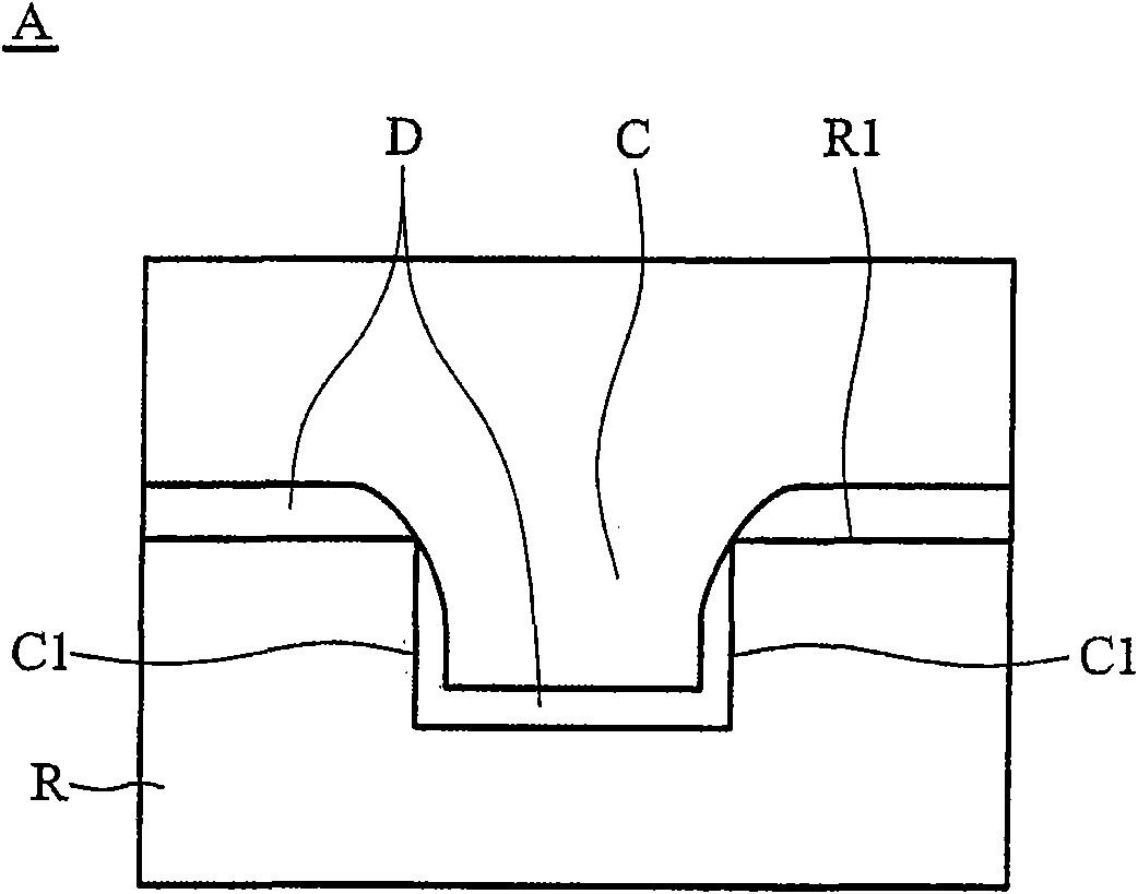
[0030] In this embodiment, there is an annular plane R1 on the periphery of the opening R2 of the focus rin...
PUM
 Abstract
Description
Claims
Application Information
 - R&D
- Intellectual Property
- Life Sciences
- Materials
- Tech Scout
- Unparalleled Data Quality
- Higher Quality Content
- 60% Fewer Hallucinations
Browse by: Latest US Patents, China's latest patents, Technical Efficacy Thesaurus, Application Domain, Technology Topic, Popular Technical Reports.
© 2025 PatSnap. All rights reserved.Legal|Privacy policy|Modern Slavery Act Transparency Statement|Sitemap|About US| Contact US: help@patsnap.com