Method of manufacturing printed circuit board base sheet

A technology for a wiring circuit substrate and a manufacturing method, which is applied in the directions of printed circuit manufacturing, circuits, printed circuits, etc., can solve problems such as poor appearance of a substrate for a wiring circuit substrate, and achieve the effect of preventing poor appearance.

Inactive Publication Date: 2010-01-13
NITTO DENKO CORP
View PDF1 Cites 5 Cited by
  • Summary
  • Abstract
  • Description
  • Claims
  • Application Information

AI Technical Summary

Problems solved by technology

When thermocompression bonding of the insulating layer and the metal layer is performed in this state, gas enters between the insulating layer and the metal layer, making the appearance of the base material for printed circuit boards poor

Method used


Image

  • Method of manufacturing printed circuit board base sheet
  • Method of manufacturing printed circuit board base sheet
  • Method of manufacturing printed circuit board base sheet

Examples


Embodiment Construction

[0022] Hereinafter, the manufacturing method of the base material for printed circuit boards which concerns on one Embodiment of this invention is demonstrated, referring drawings.

[0023] (1) Composite metal layer

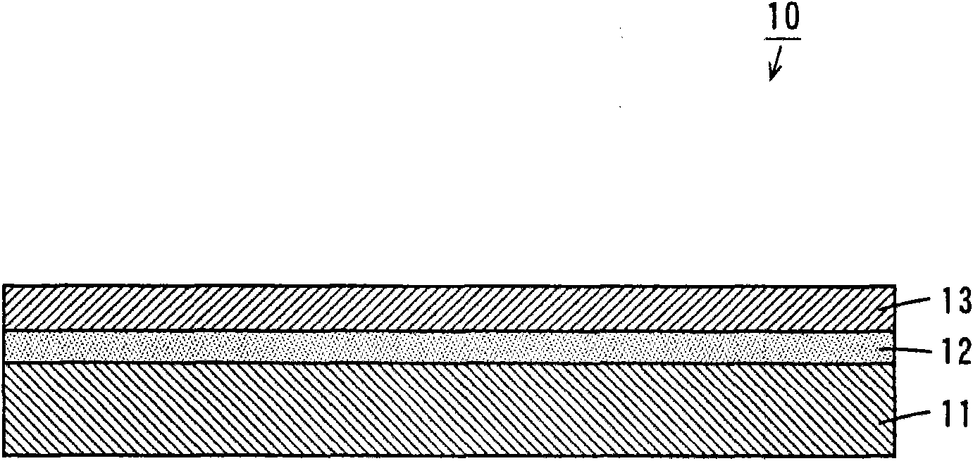
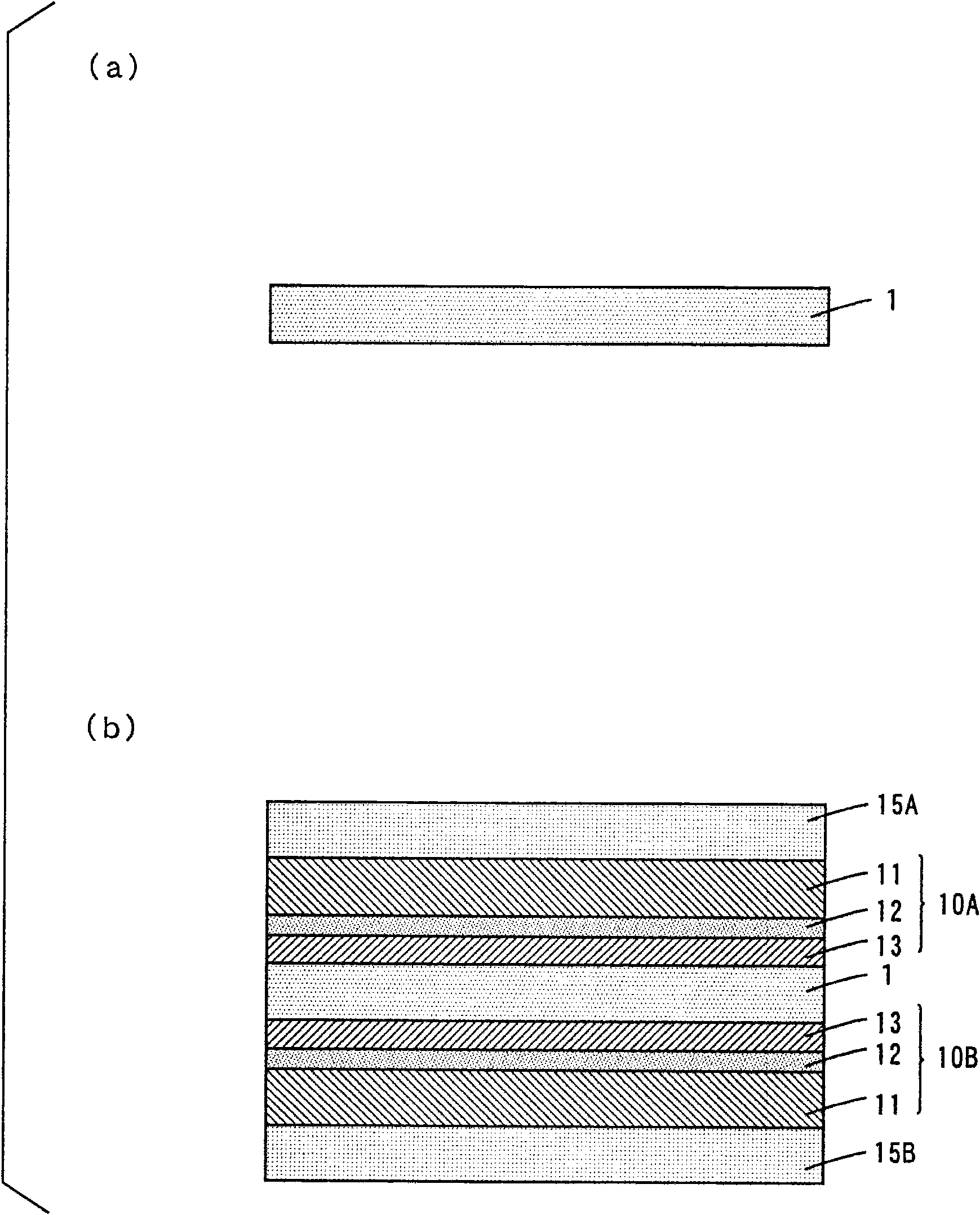
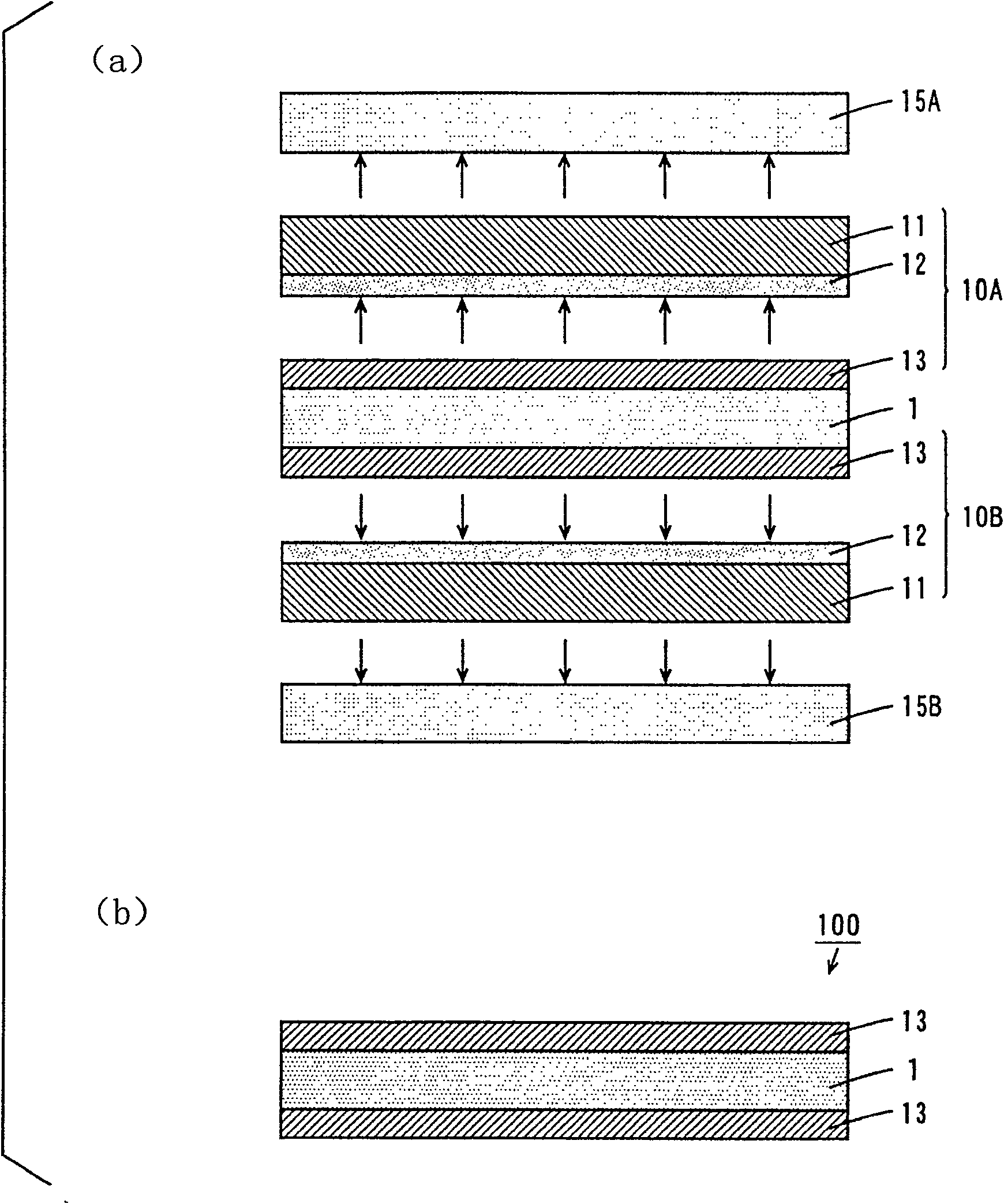
[0024] figure 1 It is a schematic sectional view of the composite metal layer used in the manufacturing method of the base material for printed circuit boards of this embodiment.

[0025] like figure 1 As shown, in the composite metal layer 10 , a metal layer 13 is laminated on a support layer 11 via a release layer 12 . The support layer 11 and the metal layer 13 are made of metal materials such as electrolytic copper foil, for example. The thickness of the support layer 11 is, for example, not less than 10 μm and not more than 150 μm, preferably not less than 15 μm and not more than 100 μm. The thickness of the metal layer 13 is, for example, 9 μm or less, preferably 1 μm or more and 5 μm or less.

[0026] The release layer 12 includes a first diffusion pr...


PUM

PropertyMeasurementUnit
thicknessaaaaaaaaaa
thicknessaaaaaaaaaa
thicknessaaaaaaaaaa

Abstract

A combined metal layer and a protective film are arranged on one surface side of an insulating layer, and a combined metal layer and a protective film are arranged on the other surface side of the insulating layer. These layers are overlapped one another to be passed between a pair of laminating rollers. In this case, a temperature with which the combined metal layers are heated by the laminating rollers is adjusted to not less than 300 DEG C. and not more than 360 DEG C. A time period during which the combined metal layers are heated by the laminating rollers is adjusted to not less than 0.1 second and not more than 0.8 second.

Description

technical field [0001] This invention relates to the manufacturing method of the base material for printed circuit boards. Background technique [0002] In recent years, electronic devices, such as digital home appliances and mobile phones, have advanced in terms of higher functionality, miniaturization, and weight reduction. Along with this, the density of the wiring pattern of the printed circuit board provided in the electronic device is increasing. [0003] When producing a printed circuit board, for example, a base material for a printed circuit board in which an insulating layer such as a resin film and a metal layer such as copper foil are laminated is used. And the wiring pattern is formed by etching the metal layer of the base material for printed circuit boards in a predetermined pattern. [0004] However, the thinning of the metal layer of the base material for printed circuit boards has been strongly desired along with the increase in the density of the wiring ...

Claims


Application Information

Patent Timeline
Patent Type & Authority Applications(China)
IPC IPC(8): H01L21/48
CPCH05K1/0393H05K3/025H05K2203/068H05K2203/0143H05K2203/1383H05K2203/1105
Inventor 徐竞雄三宅康文
Owner NITTO DENKO CORP
Why Eureka
Try Eureka