Multi-threshold field MOSFET and multi-threshold field MOSFET unit
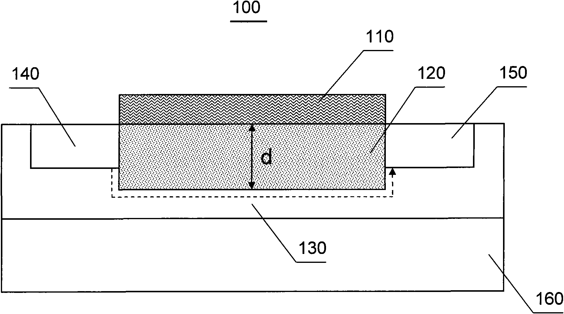
A multi-threshold, gate dielectric layer technology, applied in the direction of electrical components, transistors, circuits, etc., can solve the problems of complex process, difficult precise control, and difficult precise control of Vth, and achieve low cost, simple manufacturing process, and easy realization of changes. Effect
- Summary
- Abstract
- Description
- Claims
- Application Information
AI Technical Summary
Problems solved by technology
Method used
Image
Examples
Embodiment Construction
[0027] In order to make the object, technical solution and advantages of the present invention clearer, the present invention will be further described in detail below in conjunction with the accompanying drawings.
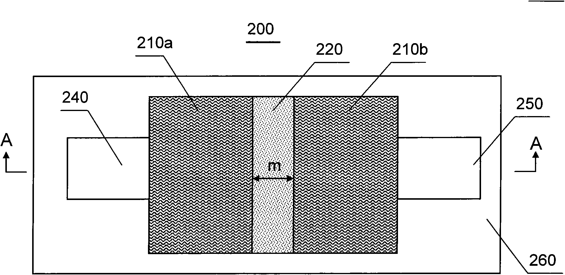
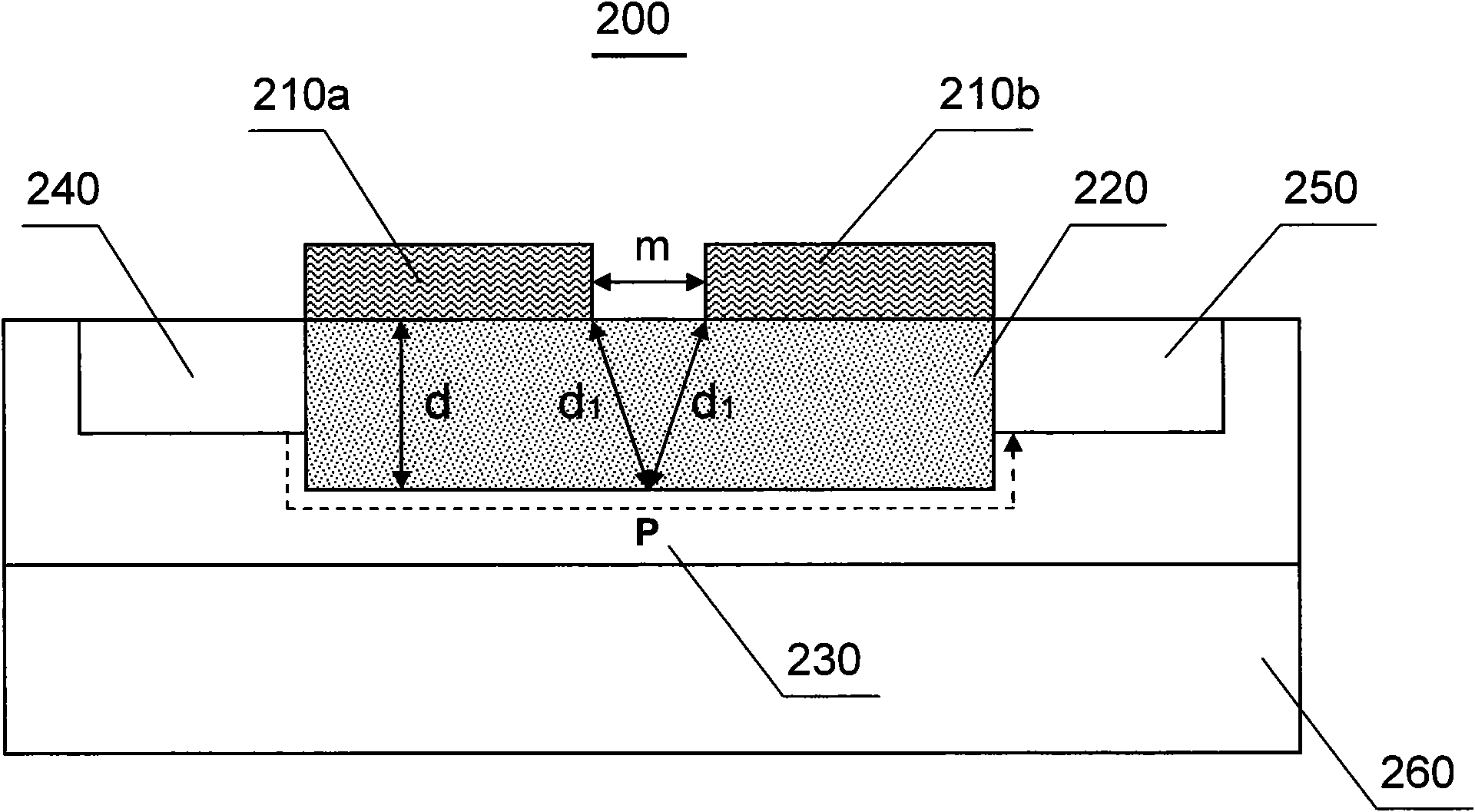
[0028] figure 2 Shown is a top view of the multi-threshold field MOSFET structure of the first embodiment of the present invention, image 3 Shown is a cross-sectional view of the multi-threshold field MOSFET structure of the first embodiment of the present invention, the cross-sectional view is figure 2 The cross-section at A-A in the middle. Such as figure 2 , image 3 As shown, the multi-threshold field MOSFET 200 includes a gate electrode, a gate dielectric layer 220, a channel region 230, a source (Source) 240, a drain (Drain) 250 and a semiconductor substrate 260, and an N-type multi-threshold field MOSFET is For example, the semiconductor substrate 260 is a P-type doped semiconductor, and the semiconductor substrate 260 is further doped with P-type t...
PUM
 Abstract
Description
Claims
Application Information


