Solder bump interconnect for improved mechanical and thermo mechanical performance

A technology of bump structure and metal under bump, which is applied in the direction of semiconductor/solid-state device components, semiconductor devices, electrical components, etc., and can solve problems such as overlap

Active Publication Date: 2010-01-27
HUATIAN TECH KUNSHAN ELECTRONICS
View PDF4 Cites 45 Cited by
  • Summary
  • Abstract
  • Description
  • Claims
  • Application Information

AI Technical Summary

Problems solved by technology

This results in significant overlap of the UBM 305 over the device pad 302

Method used


Image

  • Solder bump interconnect for improved mechanical and thermo mechanical performance
  • Solder bump interconnect for improved mechanical and thermo mechanical performance
  • Solder bump interconnect for improved mechanical and thermo mechanical performance

Examples


Embodiment Construction

[0041] The following description and drawings illustrate specific embodiments sufficient to enable a person skilled in the art to practice the systems and methods described herein. Other embodiments may incorporate structural, logical processing and other changes and are also intended to fall within the scope of this disclosure. Examples represent possible variations only.

[0042] Elements that implement various embodiments of the present systems and methods are described below. Many elements are configurable using known structures. It should also be understood that the techniques of the present systems and methods can be implemented using a variety of techniques.

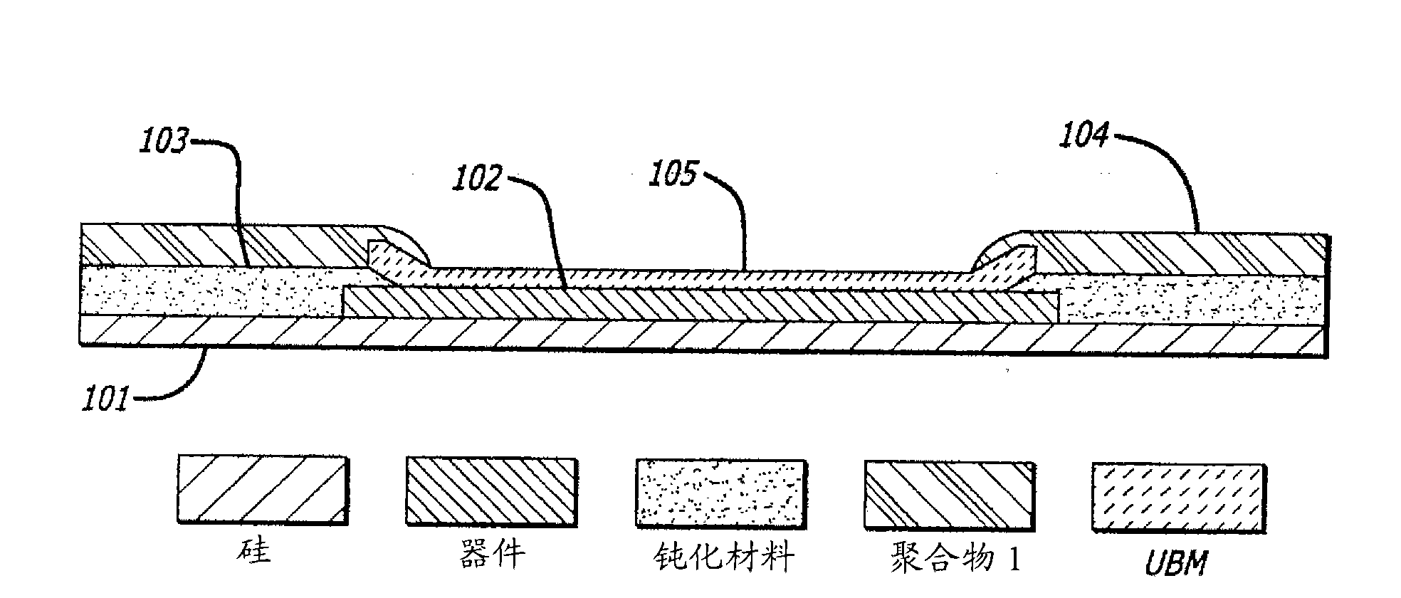
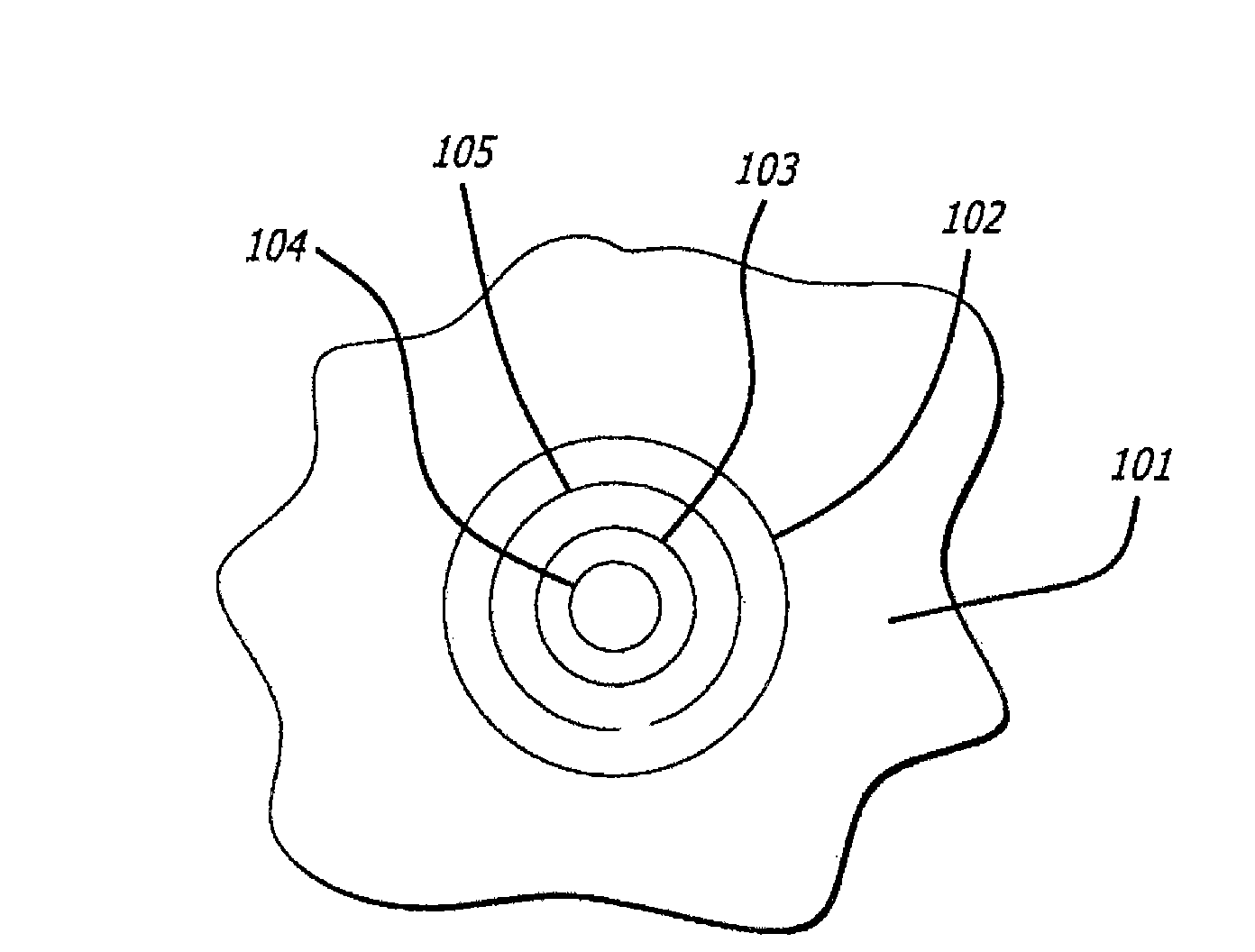
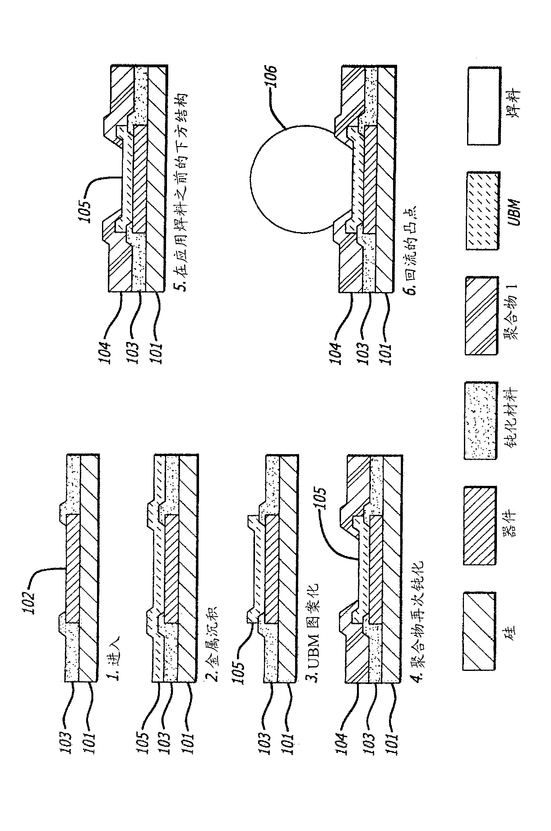
[0043] Disclosures of specific embodiments of solder bump interconnect structures with improved thermomechanical strength and drop test performance are presented below. Semiconductor device packages are typically implemented as chip-scale or wafer-level packages, eg, for chip-on-board assembly applications, or ...


PUM


Abstract

An apparatus and method for a semiconductor package including a bump on input-output (IO) structure are disclosed involving a device pad, an under bump metai pad (UBM), a polymer, and a passivation layer. The shortest distance from the center of the device pad to its outer edge, and the shortest distance from the center of the UBM to its outer edge are in a ratio from 0.5:1 to 0.95:1. Also, the shortest distance from the center of the polymer to its outer edge, and the shortest distance from the center of the UBM to its outer edge are in a ratio from 0.35:1 to 0.85:1. Additionally, the shortest distance from the center of the passivation layer to its outer edge, and the shortest distance from the center of the UBM to its outer edge are in a ratio from 0.35:1 to 0.80:1.

Description

[0001] related application [0002] This application claims priority and benefit to U.S. Provisional Application Serial No. 60 / 913,337, filed April 23, 2007, and U.S. nonprovisional Application Serial No. 12 / 107,009, filed April 21, 2008, by reference The full text of the two is combined here. US Provisional Application Serial No. 60 / 913,337 is related to PCT Patent Application Serial No. PCT / US05 / 39008 filed October 28, 2005, which is hereby incorporated by reference in its entirety. PCT / U505 / 39008 relates to and claims the benefit of US Provisional Patent Application Serial No. 60 / 623,200, filed October 28, 2004, which is hereby incorporated by reference in its entirety. [0003] This application includes material that is subject to copyright protection. The copyright owner has no objection to the facsimile reproduction by anyone of the patent disclosure document as it appears in the Patent and Trademark Office files or records, but otherwise reserves all copyright rights wh...

Claims


Application Information

Patent Timeline
Patent Type & Authority Applications(China)
IPC IPC(8): H01L21/60
CPCH01L2224/05541H01L2924/01032H01L2224/05164H01L2224/48844H01L2224/13022H01L24/05H01L2224/05155H01L24/03H01L2224/05555H01L2224/48666H01L2924/10271H01L2224/05567H01L2924/01022H01L2224/0401H01L23/3171H01L2924/01028H01L2924/01013H01L2224/0235H01L2924/01003H01L2224/13006H01L2224/05124H01L2924/3011H01L2224/1148H01L2224/48647H01L2224/05166H01L2224/0239H01L2924/01033H01L2224/05073H01L2924/01074H01L2924/01078H01L2224/05022H01L2224/48847H01L2924/12044H01L2924/01023H01L2924/01046H01L2224/48866H01L2924/01082H01L2224/13007H01L24/13H01L2224/48644H01L2224/0558H01L24/02H01L2224/05666H01L2924/01029H01L2924/00013H01L2924/014H01L2224/05554H01L2924/01024H01L2224/45147H01L2224/05572H01L2224/05644H01L2224/0345H01L2924/01047H01L2224/0346H01L23/562H01L2924/01079H01L2224/05647H01L2924/14H01L2924/01006H01L23/3192H01L2924/10329H01L2924/10253H01L2924/01014H01L2224/131H01L2924/01075H01L2224/45144H01L2224/13021H01L2924/01015H01L2224/04042H01L2924/351H01L2224/05548H01L2224/02126H01L2924/00014H01L2924/00015H01L2224/13099H01L2924/00
Inventor 雷南特·阿尔瓦拉多陆原理查德·雷德本
Owner HUATIAN TECH KUNSHAN ELECTRONICS
Why Eureka
Try Eureka