
Mems probe fabrication on a reusable substrate for probe card application

A technology of micro-electromechanical and probe card, applied in the field of micro-electromechanical, can solve the problems of unevenness, uneven outline, lack of smooth transition and so on

Inactive Publication Date: 2010-02-10
WINMEMS TECH
View PDF0 Cites 14 Cited by
  • Summary
  • Abstract
  • Description
  • Claims
  • Application Information

AI Technical Summary

Problems solved by technology

As a result, the final probe structure, including the probe springs, tends to have a jagged and uneven profile with a lack of smooth transitions between layers

Method used


Image

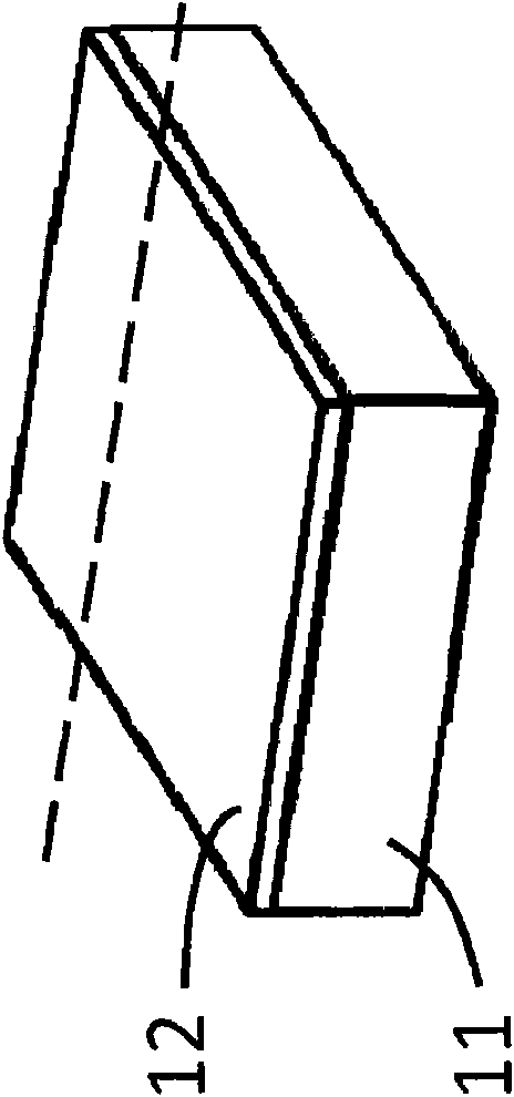
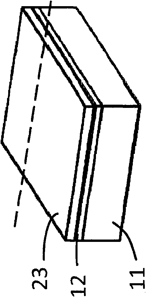
  • Mems probe fabrication on a reusable substrate for probe card application
  • Mems probe fabrication on a reusable substrate for probe card application
  • Mems probe fabrication on a reusable substrate for probe card application

Examples


Embodiment Construction

[0029] In the description below, numerous details are set forth. However, it will be readily understood by those skilled in the art that the present invention may be practiced without these specific details. In some instances, well-known structures and devices are shown in block diagram form rather than in specific detail in order to avoid obscuring the present invention.

[0030] The term "MEMS probe" herein refers to a probe made by microelectromechanical technology. It should be understood that the techniques described herein can also be applied to other MEMS components (such as mechanical components, optical components, electrical components, etc.). Typically, the dimensions of MEMS parts range from 10×10×10 microns to 5000×5000×5000 microns. Examples of MEMS components include a probe, a laser module, optical lenses, microgears, microresistors, microcapacitors, microinductors, microdiaphragms, microrelays, microsprings, waveguides, microgrooves, and the like.

[0031] ...


PUM


Abstract

A Micro-Electro-Mechanical-Systems (MEMS) probe is fabricated on a substrate for use in a probe card. The probe has a bonding surface to be attached to an application platform of the probe card. The bonding surface is formed on a plane perpendicular to a surface of the substrate. An undercut is formed beneath the probe for detachment of the probe from the substrate.

Description

technical field [0001] The present invention relates to micro-electro-mechanical systems (MEMS), and more particularly to the formation of micro-electro-mechanical probes. Background technique [0002] Micro-Electro-Mechanics (MEMS) integrates mechanical elements, sensors, actuators, and electronics on a shared substrate (such as a silicon substrate) through microfabrication technology. Electronic devices are fabricated using an integrated circuit (IC) process sequence (eg, CMOS process, bipolar process, or BICMO process), while micromechanical components are fabricated using a compatible "micromachining" process, These "micromachining" processes create mechanical and electromechanical devices by selectively etching away portions of silicon wafers or adding new structural layers. [0003] A MEMS device consists of tiny structures with dimensions on the micron scale (one millionth of a meter). Significant parts of MEMS technology have been adopted from integrated circuit (I...

Claims


Application Information

Patent Timeline
IPC IPC(8): G01R1/067B81B7/02B81C1/00H01L21/66B81C5/00
CPCG01R3/00G01R1/06744G01R1/07342G01R1/06716G01R1/06727Y10T29/49204G01R1/067H01L22/00
Inventor 徐曾洋林宝九
Owner WINMEMS TECH
Learn More