
Method for manufacturing back side illumination image sensor

A technology of image sensor and manufacturing method, applied in semiconductor/solid-state device manufacturing, electric solid-state device, semiconductor device, etc., can solve problems such as complex process, difficult to provide ohmic contact between metal wire and photodiode, metal wire short circuit, etc., to achieve The effect of reducing manufacturing costs

Inactive Publication Date: 2011-11-09
DONGBU HITEK CO LTD
View PDF0 Cites 0 Cited by
  • Summary
  • Abstract
  • Description
  • Claims
  • Application Information

AI Technical Summary

Problems solved by technology

However, at this time, it may be difficult to properly contact the metal wire to the photodiode, and it may be difficult to provide an ohmic contact between the metal wire and the photodiode
In addition, according to the existing technology, the metal line connected to the photodiode may be short-circuited
Although research has been devoted to preventing short-circuit defects between metal lines, the problem is that complex processes are required

Method used


Image

  • Method for manufacturing back side illumination image sensor
  • Method for manufacturing back side illumination image sensor
  • Method for manufacturing back side illumination image sensor

Examples


Embodiment Construction

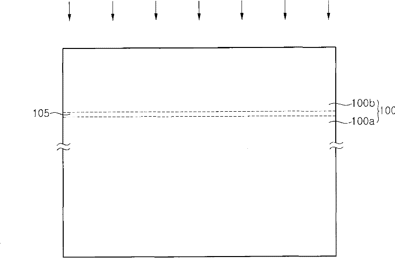
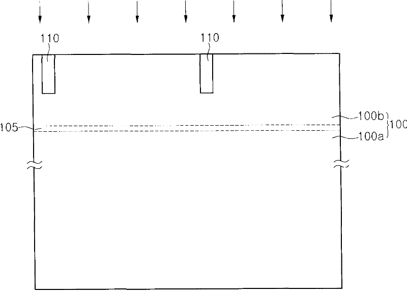
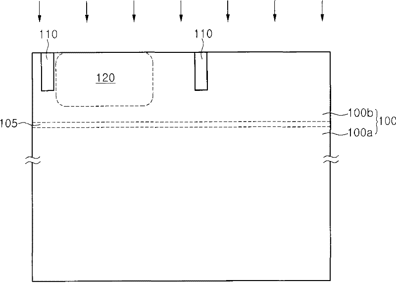
[0026] Hereinafter, a method of manufacturing a backside illuminated image sensor will be described in detail with reference to the accompanying drawings.

[0027] In the description of embodiments, it will be understood that when a layer (or film) is referred to as being 'on' another layer or substrate, it can be directly on another layer or substrate, or intervening layers may also be present. Further, it will be understood that when a layer is referred to as being "under" another layer, it can be directly under, and one or more intervening layers may also be present. In addition, it will also be understood that when a layer is referred to as being "between" two layers, it can be the only layer between the two layers, or one or more intervening layers may also be present.

[0028] Figure 1A to Figure 1C The operation of forming the ion implantation layer 105 according to some embodiments of the present invention is exemplarily shown.

[0029] see Figure 1A , the ion imp...


PUM


Abstract

Provided are methods for manufacturing a back side illumination image sensor. In one method, an ion implantation layer is formed in an entire region of a front side of a first substrate. A device isolation region is formed in the front side of the first substrate to define a pixel region. A light sensing unit and a readout circuitry are formed in the pixel region. An interlayer insulating layer and a metal line are formed on the first substrate. A second substrate is bonded to the front side of the first substrate on which the metal line is formed. A lower side of the first substrate under the ion implantation region is removed such that the light sensing unit is available at the backside of the first substrate.

Description

technical field [0001] The invention relates to a method of manufacturing a backside illuminated image sensor. Background technique [0002] An image sensor is a semiconductor device that converts an optical image into an electrical signal. Image sensors are generally classified as Charge Coupled Device (CCD) image sensors or Complementary Metal Oxide Semiconductor (CMOS) image sensors (CIS). [0003] In prior art image sensors, ion implantation is used to form photodiodes in the substrate. Since the size of the photodiode is increasingly reduced in order to increase the number of pixels without increasing the chip size, the area of ​​the light receiving portion is also reduced, resulting in lowered image quality. [0004] Furthermore, since the stack height does not decrease as much as the area of ​​the light receiving portion, the number of photons incident to the light receiving portion also decreases due to light diffraction called Airy disk. [0005] As an option to ...

Claims


Application Information

Patent Timeline
Patent Type & Authority Patents(China)
IPC IPC(8): H01L21/82H01L27/146
CPCH01L27/14634H01L27/1469H01L27/14689H01L27/14636H01L27/1464H01L27/146
Inventor 黄俊沈喜成
Owner DONGBU HITEK CO LTD
Learn More