Check patentability & draft patents in minutes with Patsnap Eureka AI!

Dry etching method

A dry etching and etching technology, applied in electrical components, semiconductor/solid-state device manufacturing, circuits, etc., can solve problems such as poor electroplating, the cost of setting the pulse generator, and the change in the width of the through hole 15.

Active Publication Date: 2010-02-17
ULVAC INC
View PDF2 Cites 2 Cited by
  • Summary
  • Abstract
  • Description
  • Claims
  • Application Information

AI Technical Summary

Problems solved by technology

Therefore, for example, when an interlayer wiring (contact hole) is formed by forming a conductive plated film on the side walls of the through hole 15 and the recess 16, there is a problem that it is easy to be damaged due to plating that occurs at the formation site of the notch 17. Bad lead to open circuit
[0009] In addition, in the conventional dry etching method, when the insulating layer 13 is etched, the collision of ions in the plasma not only occurs in the surface area of ​​the insulating layer 13 exposed from the through hole 15, but also Occurs on the side wall of the through hole 15, therefore, there is also the following problem: With the formation of the recess 16, the formation width (or diameter) of the through hole 15 will change, so that high-precision microfabrication cannot be performed.
However, in this structure, the installation cost of peripheral equipment such as a pulse generator is required
In addition, since the size of the notch also changes depending on the depth or formation width (diameter) of the through hole, etc., there is a problem that the control is complicated.

Method used


Image

  • Dry etching method
  • Dry etching method
  • Dry etching method

Examples


Embodiment Construction

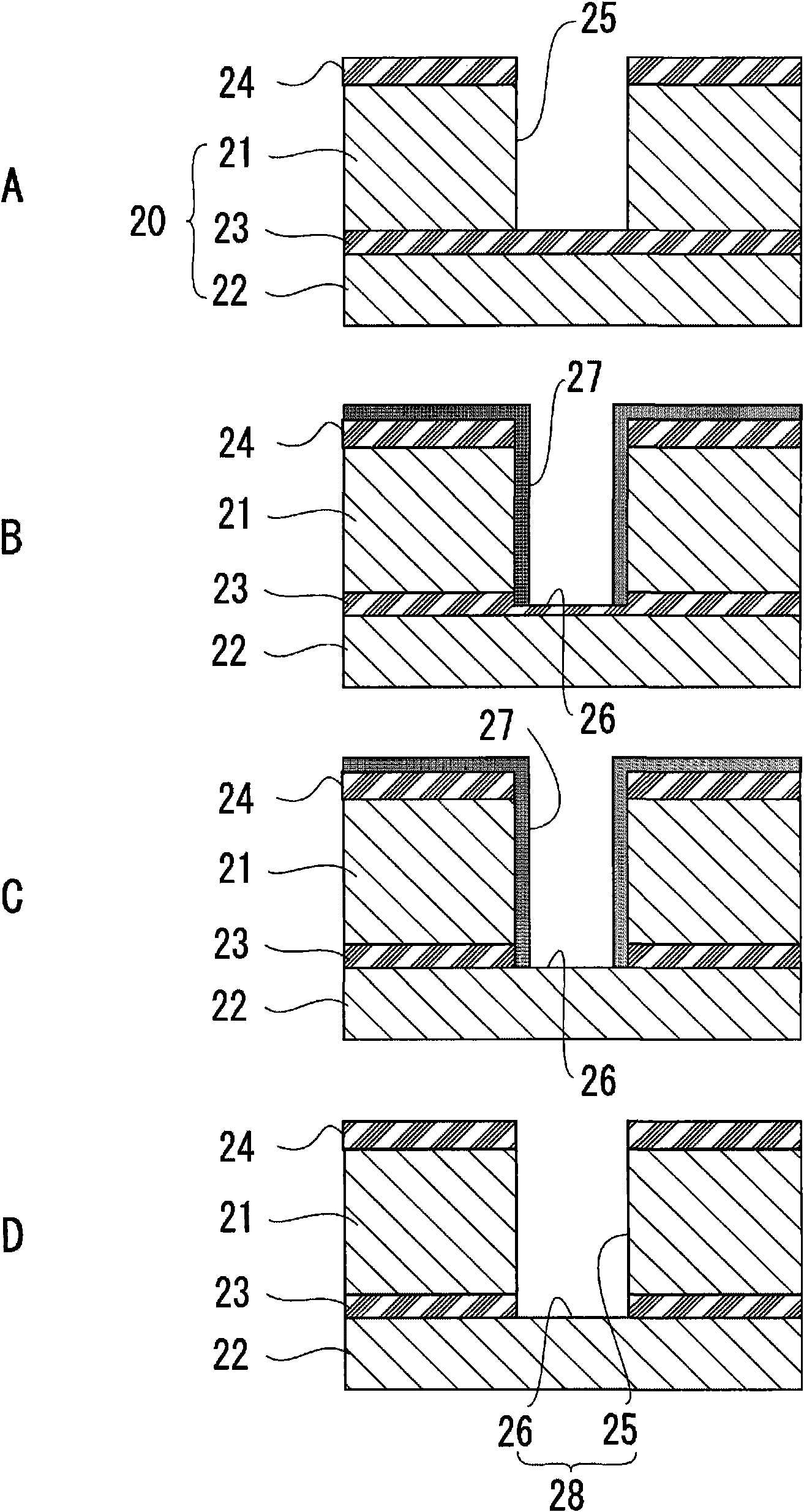
[0024] Below, refer to Figure 1 to Figure 6 A first embodiment of the present invention will be described.

[0025] A dry etching method according to an embodiment of the present invention includes: preparing a substrate in which a semiconductor layer is formed on an insulating layer made of silicon oxide.

[0026] A via hole is formed on the semiconductor layer. A recess is formed on the insulating layer by etching a region of the insulating layer exposed through the through hole, and at the same time, a resin film is formed on a side wall of the through hole and the recess. .

[0027] In the dry etching method, the recess is formed on the insulating layer, and the resin film is formed on sidewalls of the through hole and the recess. By forming the resin film on the side wall of the recess, it is possible to protect the side wall of the recess from the impact of ions in the plasma, and prevent the generation of cracks on the side wall of the recess. In addition, by formi...


PUM

PropertyMeasurementUnit
Thicknessaaaaaaaaaa

Abstract

To provide a dry etching method not causing any notch in the insulating layer and realizing high-accuracy microfabrication. ¢MEANS FOR SOLVING PROBLEMS! According to the dry etching method, a substrate where a semiconductor layer (21) is formed on a silicon oxide insulating layer (23) is prepared, a through hole (25) is formed in the semiconductor layer (21), the region of the insulating layer (23) exposed in the through hole (25) is etched to form a recess (26) in the insulating layer (23), and a resin film (27) is formed on the side wall of the through hole (25) and the side wall of the recess (26). Since the resin film (27) is formed on the side wall of the recess (26), the side wall of the recess (26) is protected from collision of ions in the plasma, and no notch in the side wall of the recess is formed. Further, since the resin film (27) is formed on the side wall of the through hole (25), the side wall of the through hole (25) is protected from collision of ions in the plasma. Thus, variation of the hole shape of the through hole (25) is prevented.

Description

technical field [0001] The invention relates to a dry etching method of a substrate, the insulation layer of the substrate is provided with a semiconductor layer. Background technique [0002] In recent years, SOI (Silicon On Insulator) substrates have been widely used in the manufacture of semiconductor storage elements and MEMS (Micro-Electro-Mechanical System). This SOI substrate has a structure in which an insulating layer made of a silicon oxide film is sandwiched between silicon substrates. The silicon substrate located on the upper side and the insulating layer located in the middle are processed by dry etching (plasma etching) to form holes (contact holes) and grooves (grooves) of prescribed shapes, or active spaces for active elements (for example, refer to The following patent document 1). [0003] Figure 8 A to C among them schematically show an example of processing an SOI substrate. The SOI substrate 101 includes: a first semiconductor layer 11 made of a sil...

Claims


Application Information

Patent Timeline
IPC IPC(8): H01L21/3065
CPCH01L21/3065H01L21/31116H01L21/311
Inventor 森川泰宏邹红罡
Owner ULVAC INC
Features
  • R&D
  • Intellectual Property
  • Life Sciences
  • Materials
  • Tech Scout
  • Unparalleled Data Quality
  • Higher Quality Content
  • 60% Fewer Hallucinations
Learn More