

Semiconductor device and manufacturing method
一种制造方法、半导体的技术,应用在半导体/固态器件制造、半导体器件、晶体管等方向,能够解决增加图案化栅极堆叠困难度、不能适用等问题
- Summary
- Abstract
- Description
- Claims
- Application Information
AI Technical Summary
Problems solved by technology
Method used
Image

Examples
Embodiment Construction
[0029] The present invention will provide many different embodiments to implement different features of the present invention. The composition and configuration of each specific embodiment will be described below to simplify the present invention. These are examples and do not limit the present invention. In addition, "above", "on", "under" or "on" a first element formed on a second element may include that the first element is in direct contact with the second element in the embodiment, or may also include There are other additional elements between the first element and the second element so that the first element is not in direct contact with the second element. Various elements may be shown in arbitrarily different scales for clarity and simplicity of illustration.
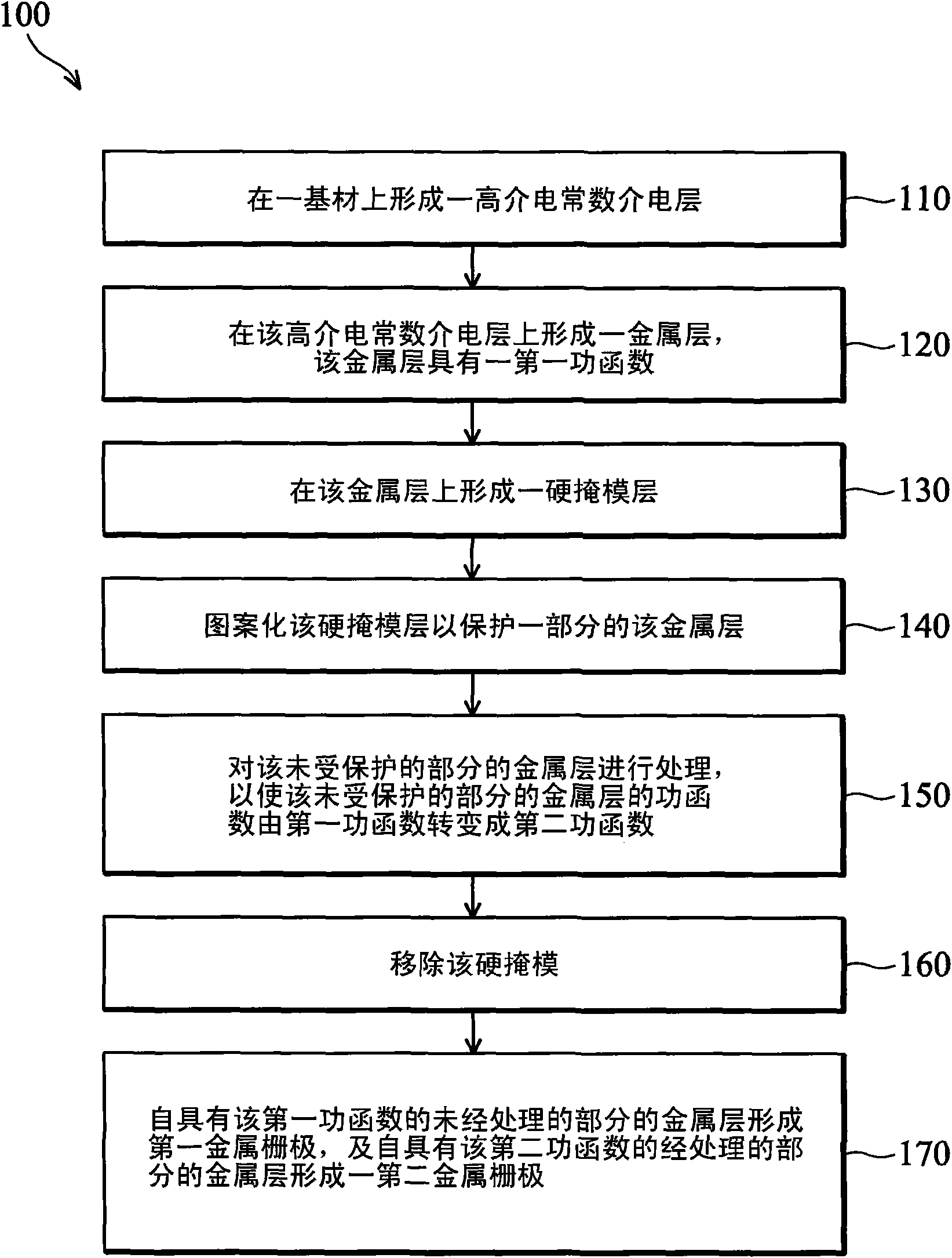
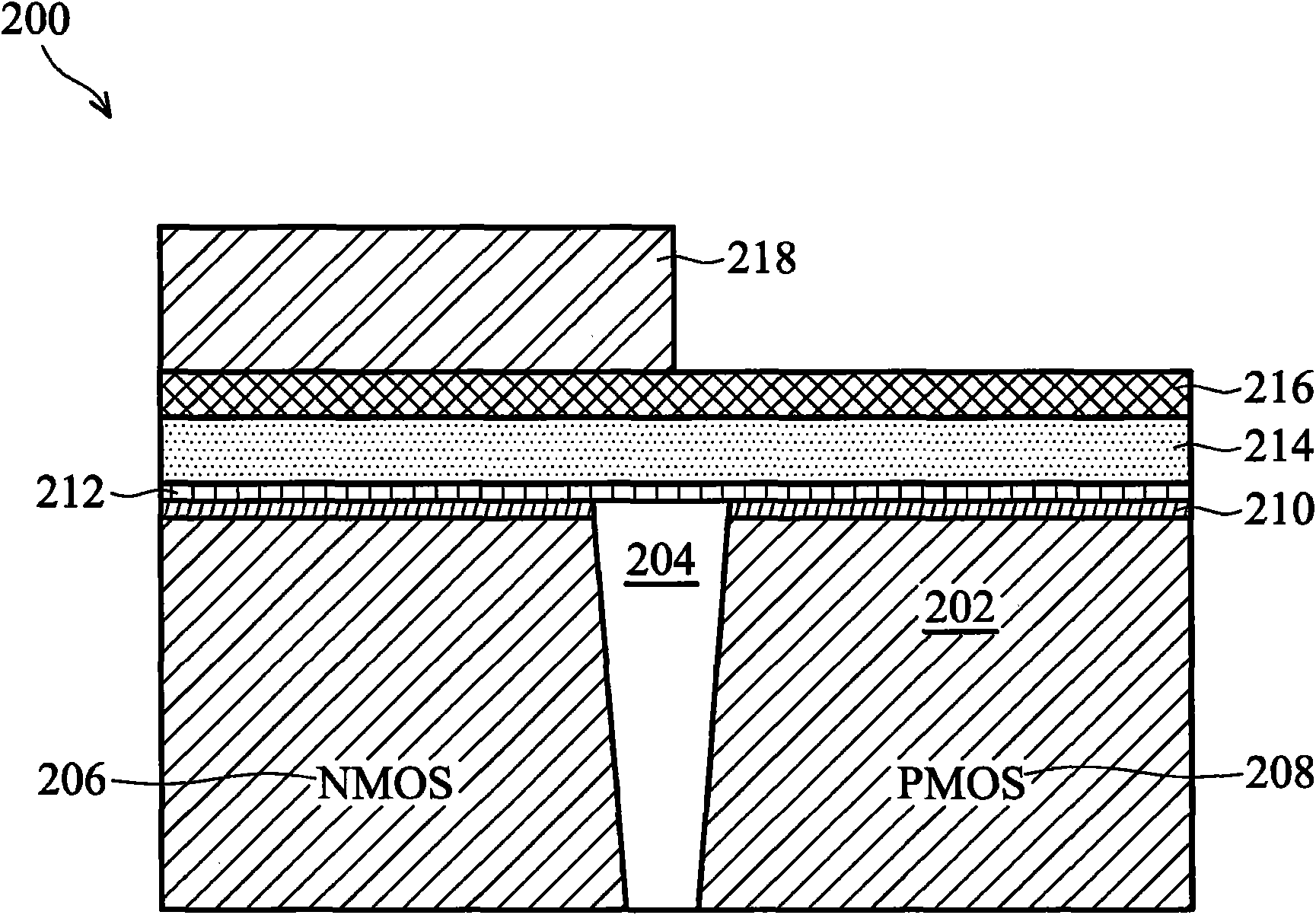
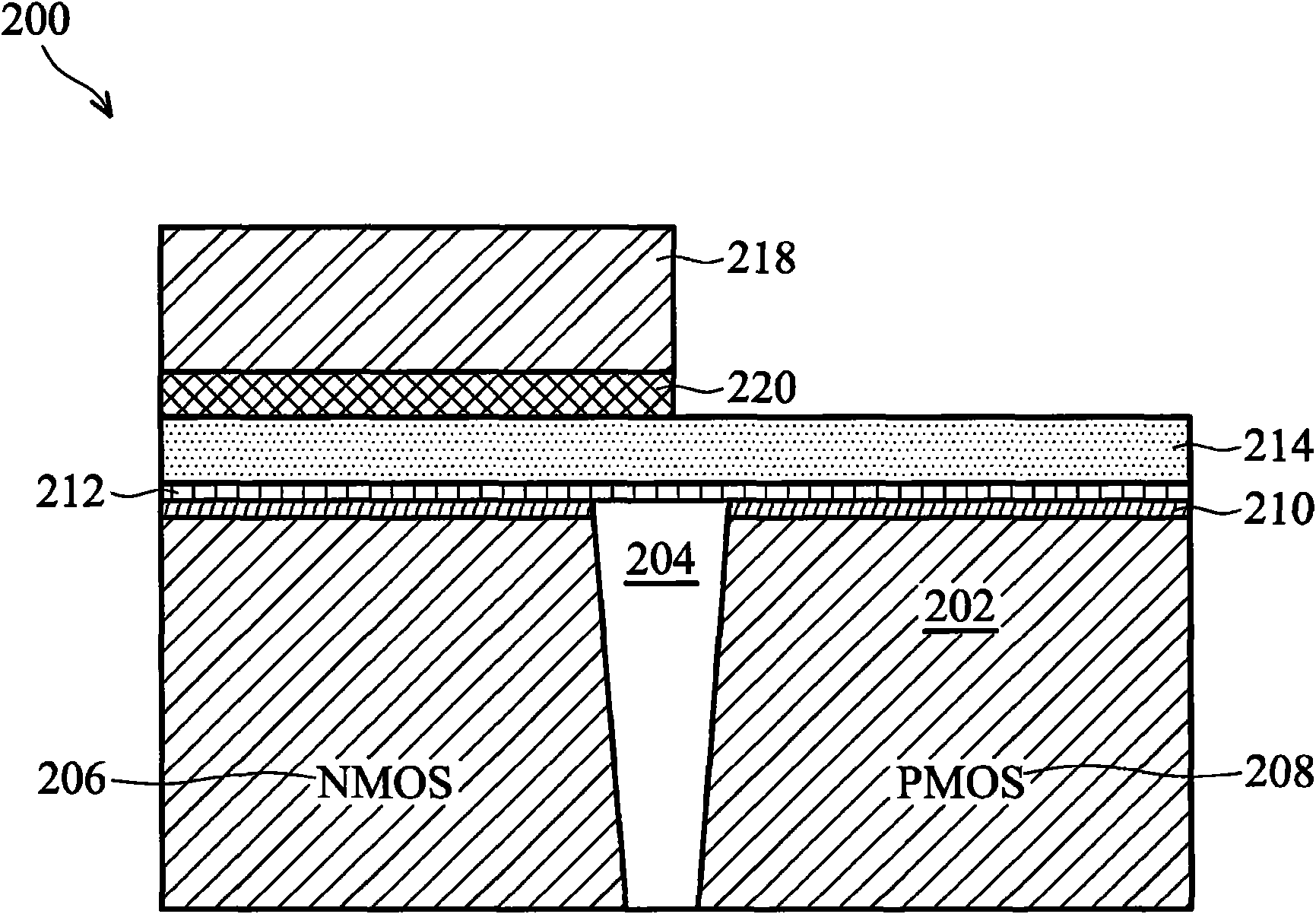
[0030] figure 1 Shown is a flowchart of a method 100 for fabricating a semiconductor device in a high-k / metal gate fabrication process. Figure 2A to Figure 2F shown as an embodiment of the invention accor...
PUM
 Abstract
Description
Claims
Application Information