Semiconductor device and manufacturing method thereof
A manufacturing method and semiconductor technology, which can be used in semiconductor/solid-state device manufacturing, semiconductor devices, electric solid-state devices, etc., and can solve problems such as performance deterioration of semiconductor devices
- Summary
- Abstract
- Description
- Claims
- Application Information
AI Technical Summary
Problems solved by technology
Method used
Image

Examples
Embodiment 1
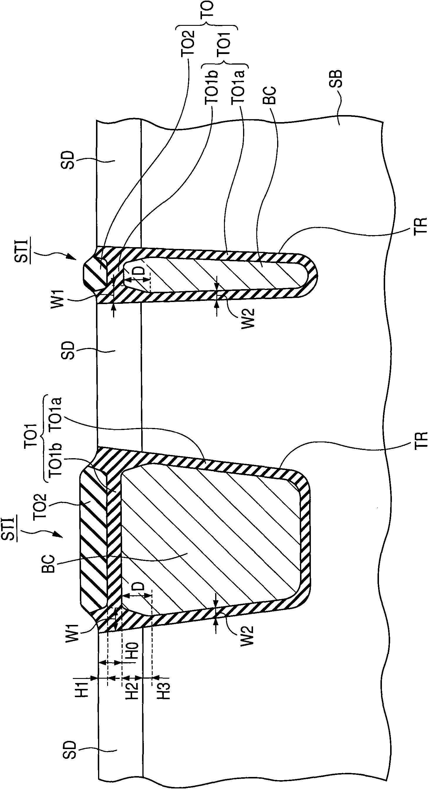
[0045] figure 1 is a cross-sectional view schematically describing the structure of the semiconductor device of Embodiment 1 of the present invention. refer to figure 1 For example, an element isolation structure STI based on a field shield STI is formed in the main surface of the semiconductor substrate SB made of silicon. Each element isolation structure STI has a trench TR, a first oxide film T01a, an embedded conductive film BC, a second oxide film T01b, and a third oxide film T02.
[0046] Trench TR is formed in the main surface of semiconductor substrate SB. The first oxide film T01a is formed to cover the wall surface of the trench TR. For example, the first oxide film T01a is a silicon oxide film formed by thermally oxidizing the surface of the semiconductor substrate SB in an atmosphere containing an active oxidizing species.
[0047] The embedded conductive film BC is embedded in the trench TR whose wall surface is covered with the first oxide film T01a and is,...
Embodiment 2
[0096] Figure 18 is a cross-sectional view schematically showing the structure of a semiconductor device according to Embodiment 2 of the present invention. refer to Figure 18 , the structure of the semiconductor device of this embodiment is the same as figure 1 The semiconductor device of Embodiment 1 shown is mainly different in the structure of the insulating film T04 on the embedded conductive film BC in each element isolation structure STI.
[0097] This insulating film T04 is, for example, a silicon oxide film, and is selectively formed on the embedded conductive film BC. The insulating film T04 has tensile stress and is further formed to provide tensile stress to the semiconductor substrate SB. In addition, in each structure STI, the insulating film T04 is joined to the silicon oxide film T03 formed on the wall surface on the trench TR. In order that the insulating film T04 is not removed by etching or the like in a subsequent step, the film thickness of the insu...
PUM
 Abstract
Description
Claims
Application Information
 - R&D
- Intellectual Property
- Life Sciences
- Materials
- Tech Scout
- Unparalleled Data Quality
- Higher Quality Content
- 60% Fewer Hallucinations
Browse by: Latest US Patents, China's latest patents, Technical Efficacy Thesaurus, Application Domain, Technology Topic, Popular Technical Reports.
© 2025 PatSnap. All rights reserved.Legal|Privacy policy|Modern Slavery Act Transparency Statement|Sitemap|About US| Contact US: help@patsnap.com