Supercharge Your Innovation With Domain-Expert AI Agents!

Method for preparing silicon germanium on insulator (SGOI) by layer transfer technology

A technology of multi-layer materials and epitaxial materials, which is applied in the field of preparing silicon-germanium-on-insulator and using layer transfer technology to prepare silicon-germanium-on-insulator materials, which can solve the problems of inability to prepare high-speed materials

Inactive Publication Date: 2013-05-22
SHANGHAI INST OF MICROSYSTEM & INFORMATION TECH CHINESE ACAD OF SCI +1
View PDF0 Cites 0 Cited by
  • Summary
  • Abstract
  • Description
  • Claims
  • Application Information

AI Technical Summary

Problems solved by technology

[0002] Manufacturing smaller-sized, higher-performance devices has always been the goal and direction of the development of the semiconductor industry. With the development of semiconductor technology, it is no longer possible to manufacture sufficiently high-speed, low-power transistors solely relying on silicon materials.

Method used


Image

  • Method for preparing silicon germanium on insulator (SGOI) by layer transfer technology
  • Method for preparing silicon germanium on insulator (SGOI) by layer transfer technology
  • Method for preparing silicon germanium on insulator (SGOI) by layer transfer technology

Examples


Embodiment 1

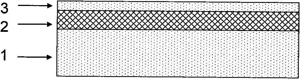
[0017] 1. Use chemical vapor deposition method to epitaxial Si sequentially on bulk silicon substrate 1-x Ge x , Si epi Two different films, where 01-x Ge x The thickness of the film is smaller than the critical thickness while ensuring the Si epi Thicker than Si 1-x Ge x Thickness (see attachment figure 1 ).

[0018] 2. Take a piece of silicon substrate material and prepare SiO on the surface of the silicon substrate by thermal oxidation, or plasma enhanced chemical vapor deposition (PECVD), or other methods 2 , SiO 2 The thickness is generally 200nm~1um.

[0019] 3. Bond the material prepared in step 1 with the material prepared in step 2 (see attached figure 2 ).

[0020] 4. Through the grinding method, the material obtained in step 3 is removed and Si 1-x Ge x Most of the adjacent bulk Si (see attached image 3 ).

[0021] 5. A chemical solution with a high Si:SiGe etching ratio including TMAH (tetramethyl ammonium hydroxide) or KOH chemical solution is used as a selective etchin...

Embodiment 2

[0025] 1. Use chemical vapor deposition method to epitaxial Si sequentially on bulk silicon substrate 1-x Ge x , Si epi Two different films, where 01-x Ge x The thickness of the film is smaller than the critical thickness while ensuring the Si epi Thicker than Si 1-x Ge x Thickness (see attachment figure 1 ).

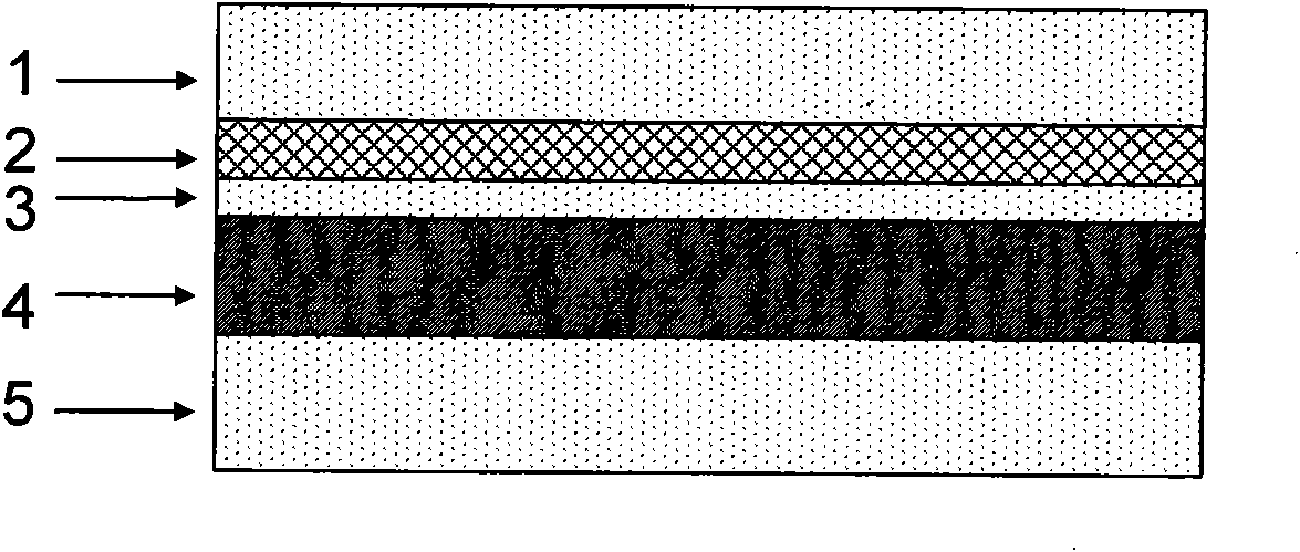
[0026] 2. Put H + Or He + 5×10 16 cm -2 ~1×10 17 cm -2 Choose the appropriate energy, and inject from the upper surface of the material prepared in step 1 into the silicon substrate layer of the epitaxial material close to Si 1-x Ge x Place of film (see attached Image 6 ), the preferred recommended dose is 6×10 16 cm -2 , The preferred implantation ion is H + .

[0027] 3. Take a piece of new silicon substrate material and prepare SiO on the surface of the silicon substrate by thermal oxidation, or plasma enhanced chemical vapor deposition (PECVD), or other methods 2 , SiO 2 The thickness is generally 200nm~1um.

[0028] 4. Bond the material prepared in step 2 with the materi...


PUM

PropertyMeasurementUnit
thicknessaaaaaaaaaa
thicknessaaaaaaaaaa

Abstract

The invention relates to a method for preparing silicon germanium on insulator (SGOI) by the layer transfer technology, comprising the following steps: extending multiple layers of materials which are in the structure of Siepi / Si1-xGex on silicon, wherein the x is more than 0 and less than 1, and the Siepi is the upper surface of the extended material; controlling the thickness of the extended thin film which is in the structure of Si1-xGex to be less than the critical thickness so as to ensure that the extended thin film is fully strained; transferring the multiple layers of materials which are in the structure of Siepi / Si1-xGex to support materials which are in the structure of SiO2 / Si by the layer transfer method to form multiple layers of materials which are in the structure of Si1-xGex / Siepi / SiO2 / Si; and annealing to enable the layer of material which is in the structure of Si1-xGex to be relaxed wherein the dislocation generated in the annealing process is mainly distributed in the layer of material which is in the structure of Siepi, so that the layer of material which is in the structure of Si1-xGex keeps high lattice quality; and continuously extending a layer of thin film which is in the structure of Si on the layer of material which is in the structure of Si1-xGex by a extending method, and keeping the layer of thin film which is in the structure of Si stressed to obtain the SGOI which is in the structure of Si / Si1-xGex / Siepi / SiO2 / Si.

Description

Technical field [0001] The invention relates to a method for preparing silicon germanium on insulator (SGOI), and more specifically to a method for preparing silicon germanium on insulator material by using layer transfer technology. It belongs to the technical field of microelectronics and solid-state electronics. Background technique [0002] The preparation of smaller size and higher performance devices has always been the goal and direction of the development of the semiconductor industry. With the development of semiconductor technology, it is no longer possible to fabricate sufficiently high-speed, low-power transistors solely relying on silicon materials. Beginning with the 90nm process, strained silicon (sSi) technology and silicon-on-insulator (SOI) technology have become two powerful tools to promote Moore's Law. Nowadays, strained silicon on insulator technology, which combines strained silicon and SOI technology, has received increasing attention from relevant scient...

Claims


Application Information

Patent Timeline
Patent Type & Authority Patents(China)
IPC IPC(8): H01L21/762H01L21/20
Inventor 张苗薛忠营张波魏星
Owner SHANGHAI INST OF MICROSYSTEM & INFORMATION TECH CHINESE ACAD OF SCI
Features
  • R&D
  • Intellectual Property
  • Life Sciences
  • Materials
  • Tech Scout
  • Unparalleled Data Quality
  • Higher Quality Content
  • 60% Fewer Hallucinations
Learn More