Luminous element

A light-emitting element, conductivity technology, used in electrical components, semiconductor devices, circuits, etc.

Active Publication Date: 2010-02-24
EPISTAR CORP
View PDF0 Cites 11 Cited by
  • Summary
  • Abstract
  • Description
  • Claims
  • Application Information

AI Technical Summary

Problems solved by technology

But from the point of view ...

Method used


Image

  • Luminous element
  • Luminous element
  • Luminous element

Examples


Embodiment Construction

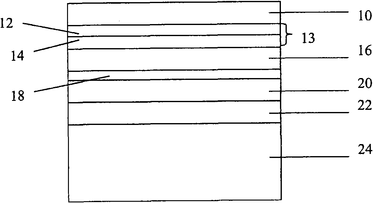
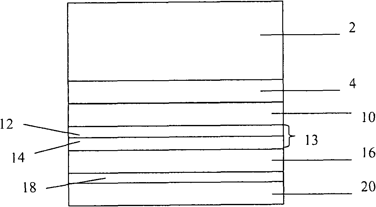
[0027] The invention discloses a light-emitting element with a tunneling layer structure and a current spreading layer and a manufacturing method thereof. In order to make the narration of the present invention more detailed and complete, refer to the following description and cooperate Figure 1 to Figure 12 icon of the .

[0028] Please refer to Figure 1 to Figure 5 , which shows a schematic diagram of the process of the light emitting device according to the first embodiment of the present invention. Please refer to figure 1 , the light-emitting element of this embodiment, such as a light-emitting diode 100, its structure includes an opaque growth substrate 24, the material of which is, for example, n-type gallium arsenide (GaAs); the epitaxial structure is sequentially grown on it as an etch stop layer ( Etching Stop Layer) 22; lower cladding layer (Lower CladdingLayer) 20, its material is, for example, n-type aluminum indium phosphide (n-type AlxInl-xP); active layer ...


PUM

PropertyMeasurementUnit
Thicknessaaaaaaaaaa
Thicknessaaaaaaaaaa

Abstract

The invention discloses a luminous element with a tunneling layer structure and a current spreading layer. The luminous element is provided with a conductive substrate which is provided with a bondinglayer; an epitaxial layer structure is arranged on the bonding layer, and comprises a first conductive semiconductor layer, an active layer and a second conductive semiconductor layer; the tunnelinglayer structure is arranged on the epitaxial layer structure, and comprises a first conductive semiconductor layer with a first dosage concentration and a second conductive semiconductor layer with asecond dosage concentration; and the current spreading layer is arranged on the tunneling layer structure.

Description

technical field [0001] The invention relates to a light-emitting element with a tunneling layer structure and a current spreading layer. Background technique [0002] Light-emitting elements such as light-emitting diodes are widely used, for example, in optical display devices, traffic signs, data storage devices, communication devices, lighting devices, and medical devices. In this technology, one of the important issues for technicians at present is how to improve the brightness of the light emitting diode. [0003] In the known technology, in order to increase the light extraction efficiency (light extraction efficiency) of the light-emitting diode formed on the p-electrode with the aluminum gallium indium phosphide (AlGaInP) material series, a p-type confinement layer (the material is p-Al 0.5 In 0.5 P) grow a material with an energy gap larger than the active layer, for example: p-Al 0.7 Ga 0.3 As or the window layer of p-GaP. In order to improve the effect of curr...

Claims


Application Information

Patent Timeline
IPC IPC(8): H01L33/00
Inventor 吕琪玮蔡孟伦
Owner EPISTAR CORP
Why Eureka
Try Eureka