Chip scale package diode component with ultra-low forward voltage and manufacture method

A technology of diode components and packaged diodes, which is applied in the direction of electrical components, semiconductor/solid-state device manufacturing, and electric solid-state devices, etc., which can solve the problems of high forward voltage, high cost, and long manufacturing process, etc. The effect of stabilizing resistance and electrical characteristics

Inactive Publication Date: 2018-01-23
FORMOSA MICROSEMI
View PDF4 Cites 0 Cited by
  • Summary
  • Abstract
  • Description
  • Claims
  • Application Information

AI Technical Summary

Problems solved by technology

[0011] 1. The original purpose of the epitaxial / diffusion layer of the N pole is to allow electrons to pass through the N pole region at a lower internal resistance when the current is forward-conducting, but the epitaxial / diffusion layer itself will generate additional internal resistance. Therefore, the forward voltage (VF) is still high
[0012] 2. The epitaxial / diffusion layer for conduction is made by means of yellow light, etching, ion implantation or diffusion on the position of the substrate or diffused silicon crystal plate relative to the N pole. The process is long and the cost is high
[0013] 3. The area other than the P and N poles is idle and unused due to the setting of the guard ring and the insulating protective layer, and the forward voltage during forward conduction will also be high
[0014] 4. The cutting line is around the periphery of the P pole and the N pole. When cutting the components, the P pole and the N pole have the problem of peripheral cracking (CHIPPING & CRACK) at the same time, which seriously affects the quality stability of the finished product of the diode element.

Method used


Image

  • Chip scale package diode component with ultra-low forward voltage and manufacture method
  • Chip scale package diode component with ultra-low forward voltage and manufacture method
  • Chip scale package diode component with ultra-low forward voltage and manufacture method

Examples


no. 1 example

[0077] For ease of description, the following embodiments are all based on N-type substrates or silicon wafers. The present invention provides a method for manufacturing a grain-sized packaged diode element with ultra-low forward voltage. The first embodiment includes the following step:

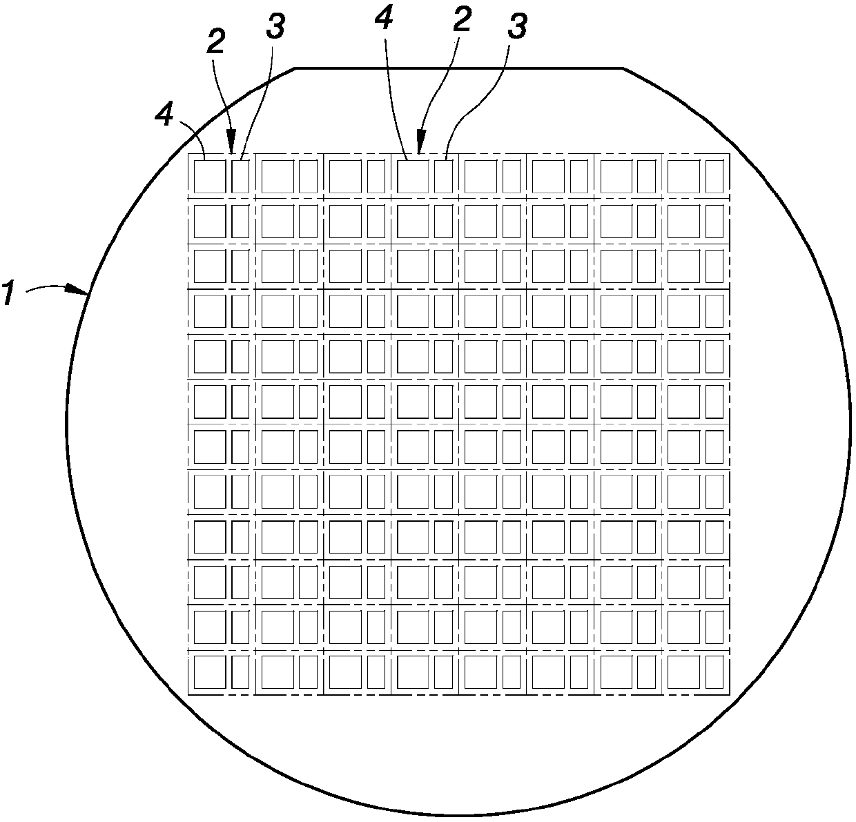
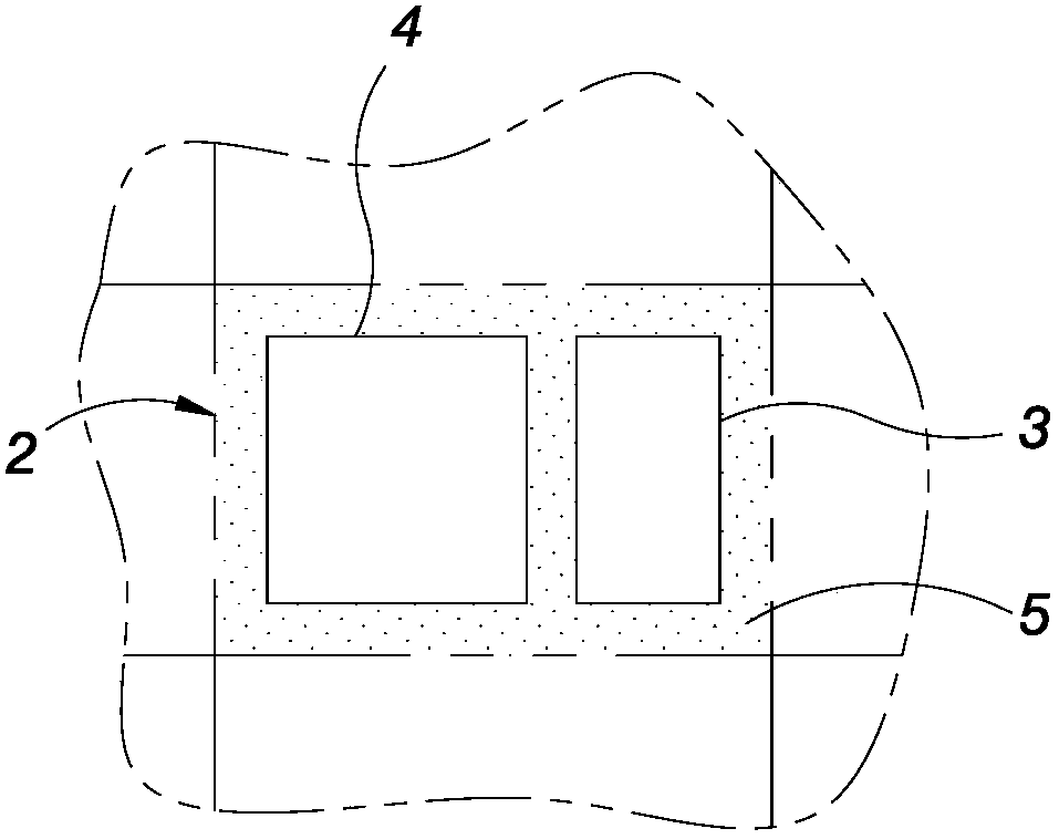
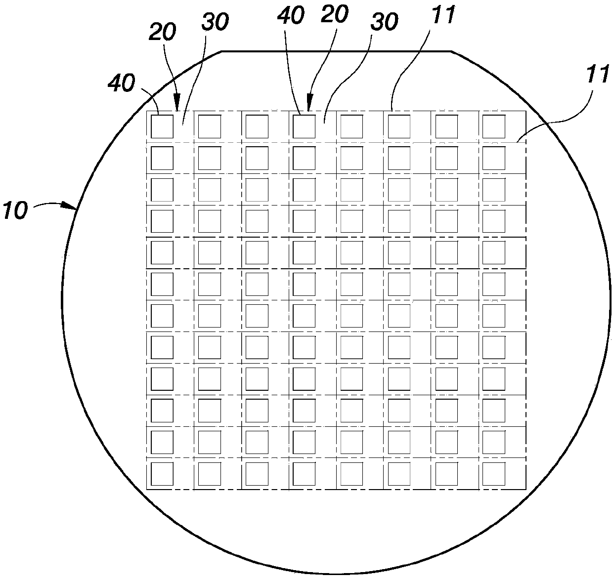
[0078] The first step: if image 3 As shown, on the front side of a substrate 10, it is divided into a plurality of diode element regions 20 according to the required size of the diode element, and a cutting line 11 is reserved on the periphery of each diode element region 20, and in each diode element region 20 The first electrode region 30 and the second electrode region 40 are arranged in the inner periphery of the diode element region 20 ; all the positions of the diode element region 20 other than the second electrode region 40 are used as the first electrode region 30 .

[0079] The second step: if Figure 4 As shown, on the position where the second electrode region 40 of each diode...


PUM


Abstract

The present invention discloses a chip scale package diode component with an ultra-low forward voltage and a manufacture method. According to the diode component, all regions except a second electrodeare directly adopted as a first electrode, and / or the front surface and back surface of the first electrode are penetrated through perforation, and are conducting, and then cutting is performed, so that a chip scale package diode component finished product with a smaller size can be obtained. Since the first electrode is not required to be conducting through an epitaxial layer or a diffusion layer, and therefore, internal resistance can be avoided, a forward voltage can be lowered. With the manufacture method adopted, a manufacture process is simplified, quality can be improved, costs can bereduced, and the diode component can be lighter, shorter and smaller.

Description

technical field [0001] The present invention relates to a chip scale package (Chip Scale Package, CSP) diode element and a manufacturing method thereof. Plate (Silicon Wafer), Diffused Layer (Diffused), Diffused Silicon Wafer (Diffused Silicon Wafer). The finished diode element has the characteristics of ultra-low forward voltage (VF), and can simplify the manufacturing process, improve the quality, reduce the cost, and make the diode element lighter, thinner and shorter, and many other advantages. Background technique [0002] Generally, semiconductor materials are used to manufacture flip-chip (CSP) diode elements in grain size packages (CSP), including epitaxial wafers (EPI Wafer) and diffused silicon wafers (Diffused Silicon Wafer). The epitaxial wafer includes a substrate (Substrate) on the back side and an epitaxial layer (Epitaxy) on the front side. The diffused silicon wafer is to set a diffused layer (Diffused) on the front and back of a layer of silicon material,...

Claims


Application Information

Patent Timeline
IPC IPC(8): H01L21/56H01L23/31
Inventor 黄文彬吴文湖林慧敏赖锡标陈建武
Owner FORMOSA MICROSEMI
Why Eureka
Try Eureka