Nitride semiconductor light emitting element and method for manufacturing nitride semiconductor

A nitride semiconductor and light-emitting element technology, applied in semiconductor devices, electrical components, nano-optics, etc., can solve the problems of deterioration of the crystal quality of the p-type semiconductor layer, hindering the p-type semiconductor layer from being p-typed, and increasing the number of manufacturing processes. The effect of improving external luminous efficiency, reducing forward voltage Vf, and alleviating deformation

Inactive Publication Date: 2010-03-31
ROHM CO LTD
View PDF3 Cites 27 Cited by
  • Summary
  • Abstract
  • Description
  • Claims
  • Application Information

AI Technical Summary

Problems solved by technology

However, when the p-type semiconductor layer is formed by a carrier gas containing hydrogen, the hydrogen atoms taken in together with the p-type impurity make it difficult to activate the p-type impurity, hindering the p-type of the p-type semiconductor layer, and the crystal quality of the p-type semiconductor layer deterioration
Therefore, after forming the p-type semiconductor layer, it is necessary to perform annealing for removing hydrogen atoms from the p-type semiconductor layer, which leads to an increase in the number of manufacturing steps.

Method used


Image

  • Nitride semiconductor light emitting element and method for manufacturing nitride semiconductor
  • Nitride semiconductor light emitting element and method for manufacturing nitride semiconductor
  • Nitride semiconductor light emitting element and method for manufacturing nitride semiconductor

Examples


Embodiment Construction

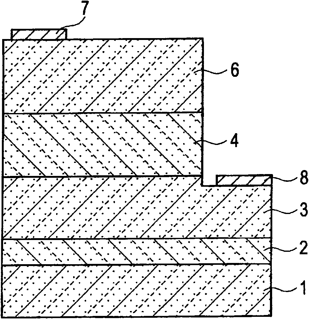
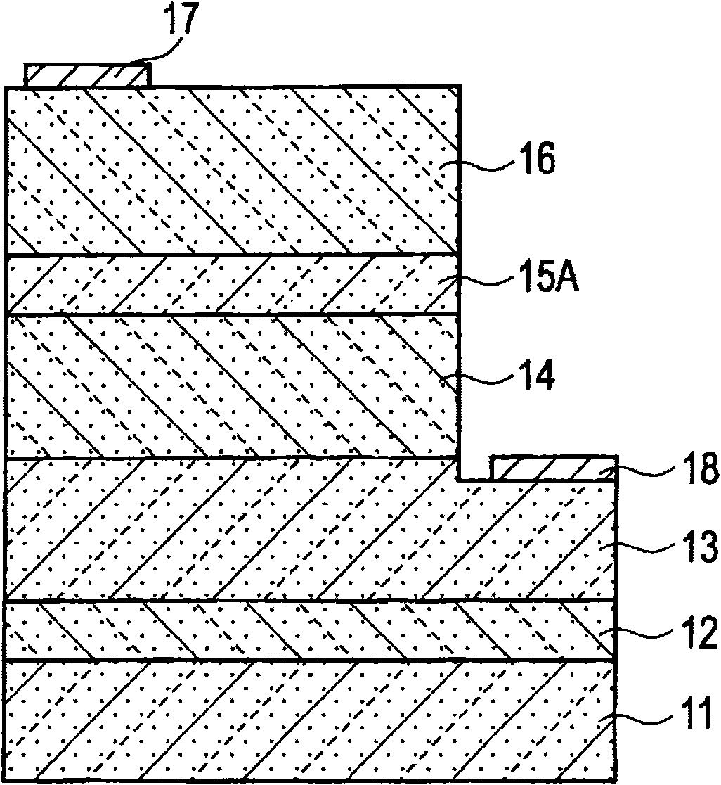
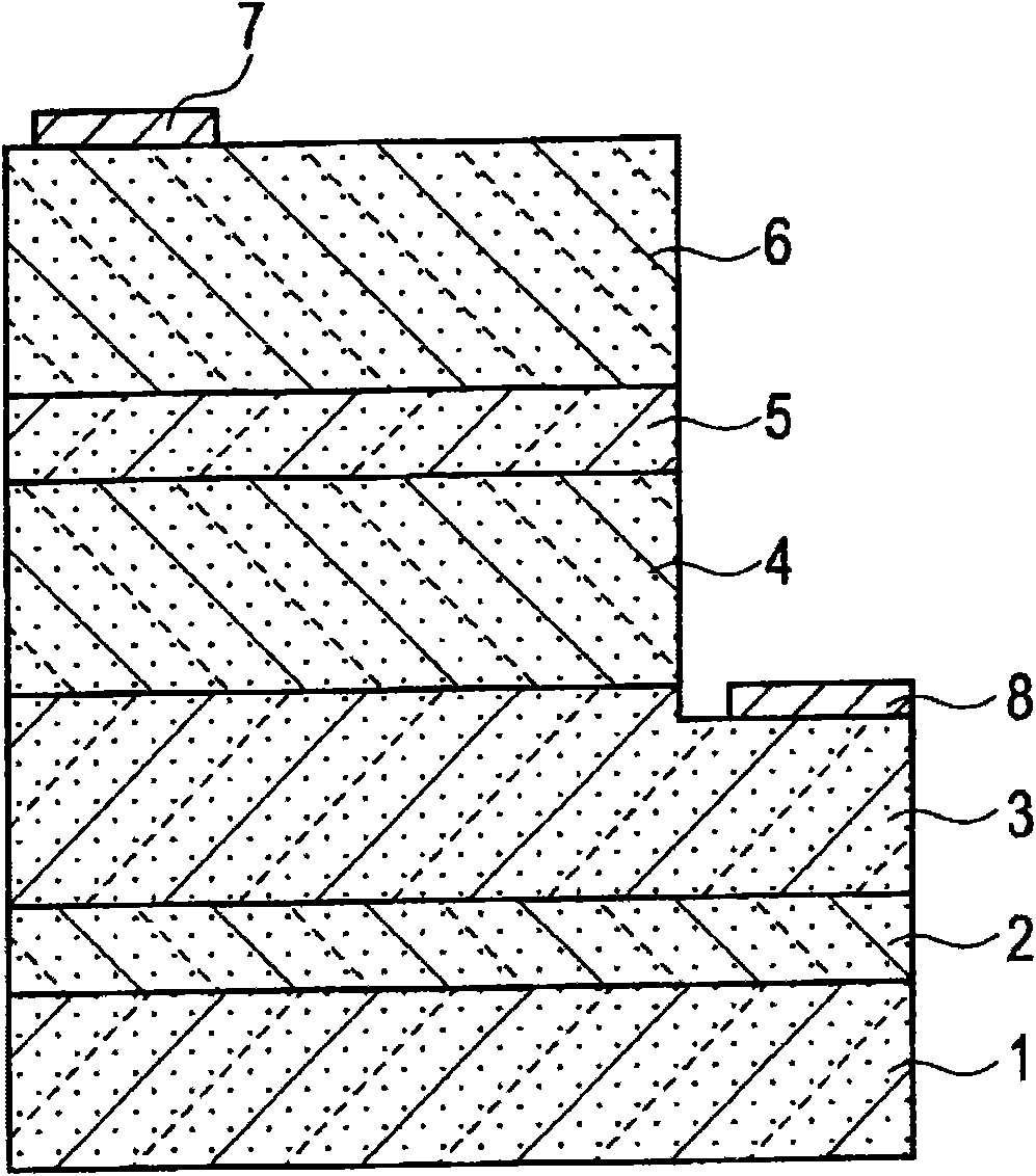
[0086] An embodiment of the present invention will be described below with reference to the drawings. figure 1 An example of the structure of the nitride semiconductor light-emitting device of the present invention is shown.

[0087] A sapphire substrate 1 is used as a growth substrate, an AlN buffer layer 2 is formed on the sapphire substrate 1, and an n-type AlGaN layer 3, an InGaN / GaN active layer 4, and a p-type GaN layer 6 are sequentially stacked thereon. Nitride semiconductors. This nitride semiconductor is formed by a known MOCVD method or the like. Nitride semiconductors are represented as AlGAAlNN quaternary mixed crystals, known as so-called III-V nitride semiconductors, which can be Al x Ga y In z N (x1+y1+z1=1, 0≤x1≤1, 0≤y1≤1, 0≤z1≤1) represents.

[0088] Mesa etching is performed until n-type AlGaN layer 3 is exposed from p-type GaN layer 6 , and n-electrode 8 is formed on the exposed surface of n-type AlGaN layer 3 . On the other hand, p-electrode 7 is for...


PUM

PropertyMeasurementUnit
thicknessaaaaaaaaaa
thicknessaaaaaaaaaa
thicknessaaaaaaaaaa

Abstract

Provided is a nitride semiconductor light emitting element having improved optical output with improved qualities, such as crystal qualities, of a nitride semiconductor laminated on an AlN buffer layer. An AlN buffer layer (2) is formed on a sapphire substrate (1), and on the buffer layer, nitride semiconductors of an n-type AlGaN layer (3), an InGaN / GaN active layer (4) and a p-type GaN layer (5)are laminated in sequence. On the surface of the n-type AlGaN layer (3), an n-electrode (7) is formed, and on the p-type GaN layer (5), a p-electrode (6) is formed. The n-type AlGaN layer (3) operates as a clad layer for confining light and carriers. The AlN buffer layer (2) is manufactured by alternately supplying an Al material and an N material at a growing temperature of 900 DEG C or higher.

Description

technical field [0001] The present invention relates to a nitride semiconductor light-emitting element and a method for manufacturing the nitride semiconductor including a laminated body made of a nitride semiconductor on an AlN buffer layer of the nitride semiconductor. Background technique [0002] The development of semiconductor elements called gallium nitride-based compound semiconductors, that is, so-called III-V nitride semiconductors (hereinafter referred to as nitride semiconductors), has been extensively carried out. Nitride semiconductors are used in blue LEDs used as light sources for lighting, backlights, etc., LEDs used for multicoloration, LDs, and the like. Since nitride semiconductors are difficult to manufacture as bulk single crystals, GaN is grown on various types of substrates such as sapphire and SiC by using MOCVD (metal organic vapor phase growth method). A sapphire substrate is particularly used as a growth substrate because it has excellent stabili...

Claims


Application Information

Patent Timeline
Patent Type & Authority Applications(China)
IPC IPC(8): H01L33/00H01L33/12H01L33/14H01L33/32
CPCH01L33/32H01L33/14H01L33/06H01L33/12H01L33/325B82Y20/00
Inventor 中西康夫中田俊次藤原彻也千田和彦园部雅之
Owner ROHM CO LTD
Why Eureka
Try Eureka