GaN device with mixed polarity

A mixed polarity and device technology, applied in semiconductor devices, electrical components, circuits, etc., can solve the problems of increasing device preparation time, deterioration of ohmic contact characteristics, and increasing process difficulty

Active Publication Date: 2016-07-20
SHIJIAZHUANG UNIVERSITY
View PDF2 Cites 8 Cited by
  • Summary
  • Abstract
  • Description
  • Claims
  • Application Information

AI Technical Summary

Problems solved by technology

However, the study found that the Ti / Al-based ohmic contact metal directly deposited on the N-polarGaN in the N-polarGaN-based HEMT cannot achieve a smaller ohmic contact resistance after high-temperature annealing, because the Al metal in the Ti / Al-based metal After high-temperature annealing, it can penetrate the Ti metal layer into GaN and combine with N to form AlN
[0005] In Ga-polarGaN, the AlN and GaN will form an AlN / GaN heterojunction similar to the AlGaN / GaN heterojunction, thereby forming a two-dimensional electron gas (2DEG) in GaN at the interface of AlN and GaN, but in the N- 2DEG will not be generated in the heterojunction formed by AlN and N-polarGaN in polarGaN, but two-dimensional hole gas (2DHG) will be formed instead, because its polarity is 180° different from that of Ga-polarGaN
However, the existence of the 2DHG is bound to make the ohmic contact characteristics worse, so that a smaller ohmic contact resistance cannot be achieved in N-polarGaN-based HEMTs.
In order to obtain a smaller ohmic contact resistance, some literature reports use ohmic regeneration to reduce the ohmic contact resistance, but this method will increase the difficulty of the process, increase the device preparation time and increase the uncertainty of the process

Method used


Image

  • GaN device with mixed polarity
  • GaN device with mixed polarity

Examples


Embodiment 1

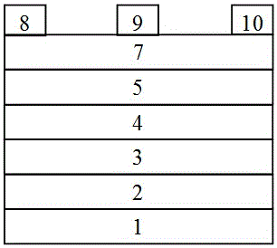
[0025] In this embodiment, the mixed polarity GaN / AlGaN Schottky barrier field effect transistor MESFET device is taken as an example, combined with the attached figure 1 Embodiments of the present invention are described in detail. The MESFET device described in this embodiment includes from bottom to top: substrate layer 1, N-polarGaN buffer layer 2, Al composition x First N-polarAl of incremental gradient x GaN layer 3, Al composition x Keep the second N-polarAl constant x GaN layer 4, Al composition x The third N-polarAl of the decreasing gradient x GaN layer 5 , Ga-polarGaN channel layer 7 ; source 8 , gate 9 and drain 10 are provided on the upper surface of Ga-polarGaN channel layer 7 .

[0026] It should be pointed out that in this embodiment: the substrate layer 1 can be a sapphire substrate, a silicon carbide substrate or a silicon substrate; the thickness of the N-polarGaN buffer layer 2 is between 1-3 μm; the Al components x Incremental Gradient Al x The GaN...

Embodiment 2

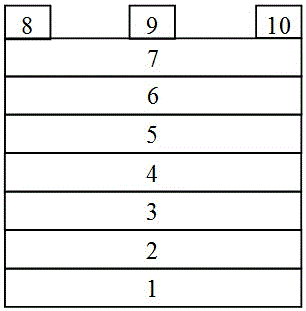
[0028] In this embodiment, the mixed-polarity GaN / AlGaN high electron mobility transistor HEMT device is taken as an example, and the attached figure 2 Embodiments of the present invention are described in detail. In this embodiment, the HEMT device includes from bottom to top: substrate layer 1, N-polarGaN buffer layer 2, Al composition x First N-polarAl of incremental gradient x GaN layer 3, Al composition x Keep the second N-polarAl constant x GaN layer 4, Al composition x The third N-polarAl of the decreasing gradient x GaN layer 5, N-polarAlN insertion layer 6, Ga-polarGaN channel layer 7; the upper surface of the Ga-polarGaN channel layer 7 is provided with a source 8, a gate 9, and a drain 10.

[0029] It should be noted that, in this embodiment: the substrate layer 1 may be a sapphire substrate, a silicon carbide substrate or a silicon substrate. The GaN buffer layer is N-polar with a thickness between 1 μm and 3 μm. The Al composition x Incremental Gradient A...


PUM


Abstract

The invention discloses a GaN device with the mixed polarity. The GaN device relates to the technical field of field effect transistors with two-dimensional carrier gas channels. The GaN device comprises a substrate layer, an N-polar GaN buffer layer, a first N-polar Alx GaN layer with a gradually increased Al component x, a second N-polar AlxGaN layer with a constant Al component x, a third N-polar AlxGaN layer with a gradually reduced Al component x, and a Ga-polar GaN channel layer. By virtue of the structure, a GaN based material with higher quality can grow epitaxially and the surface density and migration rate of 2DEG in a channel can be increased; and meanwhile a device with smaller ohmic contact resistance can be fabricated on a material with the mixed polarity by adopting a conventional Ga-polar GaN based device fabrication process.

Description

technical field [0001] The invention relates to the technical field of field effect transistors with two-dimensional carrier gas channels, in particular to a mixed-polarity GaN device. Background technique [0002] GaN-based materials have attracted the attention of researchers for their wide bandgap, high breakdown electric field, and high saturation electron drift velocity in the application fields of microelectronics and optoelectronics, and have become the frontier and hotspot of global semiconductor research. Together with SiC and other materials And known as the most promising "third-generation semiconductor materials." [0003] Due to the lack of center inversion in wurtzite-structured GaN, resulting in a very strong spontaneous polarization phenomenon, there are two types of GaN polarity (Ga-polar) and nitrogen polarity (N-polar) for wurtzite-structured GaN. Polarized GaN. Due to the opposite polarity of the two materials, there are many differences between the two...

Claims


Application Information

Patent Timeline
Patent Type & Authority Applications(China)
IPC IPC(8): H01L29/45H01L29/778
CPCH01L29/452H01L29/7783
Inventor 王现彬王颖莉刘振永于京生
Owner SHIJIAZHUANG UNIVERSITY
Why Eureka
Try Eureka