Epitaxial wafer of light emitting diode and manufacturing method thereof

A technology of light-emitting diodes and manufacturing methods, which is applied in the direction of electrical components, circuits, semiconductor devices, etc., can solve the problems of reduced internal quantum efficiency, reduced overlapping of electron and hole wave functions, etc., to improve luminous efficiency and lateral mobility , the effect of reducing electronic crowding

Inactive Publication Date: 2019-05-21
HC SEMITEK ZHEJIANG CO LTD
View PDF0 Cites 6 Cited by
  • Summary
  • Abstract
  • Description
  • Claims
  • Application Information

AI Technical Summary

Problems solved by technology

The compressive stress will generate a piezoelectric polarization electric field, which will tilt the energy band of the multi-quantum well layer, resulting in a decrease in the overlap of electron and hole wave functions, and a decrease in the internal quantum efficiency of the LED.

Method used


Image

  • Epitaxial wafer of light emitting diode and manufacturing method thereof
  • Epitaxial wafer of light emitting diode and manufacturing method thereof
  • Epitaxial wafer of light emitting diode and manufacturing method thereof

Examples


Embodiment Construction

[0031] In order to make the object, technical solution and advantages of the present invention clearer, the implementation manner of the present invention will be further described in detail below in conjunction with the accompanying drawings.

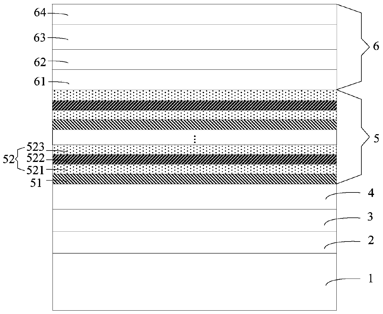
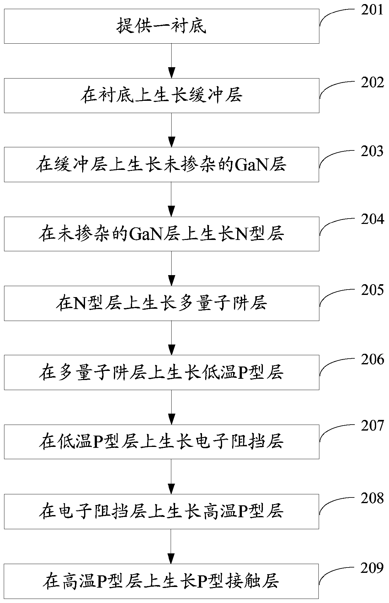
[0032] figure 1 It is a schematic structural diagram of a light-emitting diode epitaxial wafer provided by an embodiment of the present invention, as shown in figure 1 As shown, the LED epitaxial wafer includes a substrate 1 , and a buffer layer 2 , an undoped GaN layer 3 , an N-type layer 4 , a multi-quantum well layer 5 and a P-type layer 6 stacked on the substrate 1 in sequence. The multi-quantum well layer 5 is a multi-period superlattice structure, and each superlattice structure includes a quantum well layer 51 and a quantum barrier layer 52 .

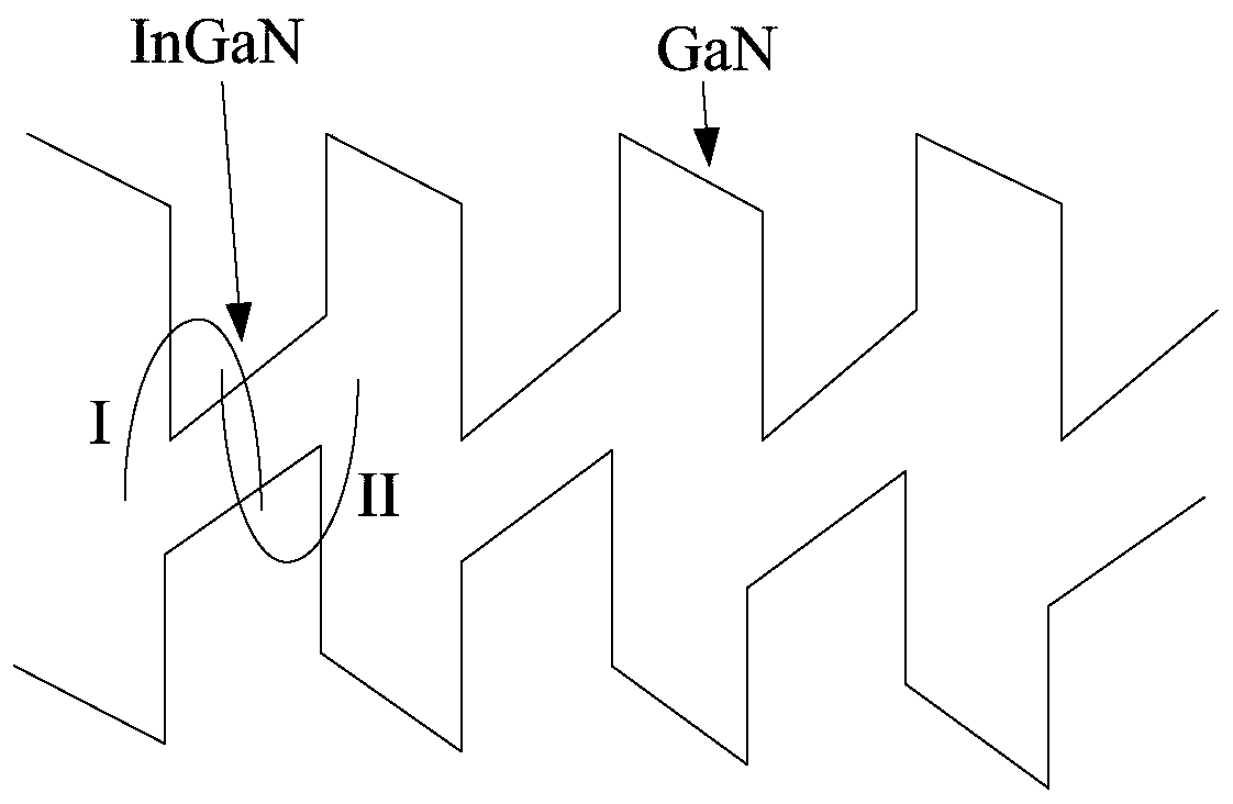
[0033] The quantum well layer 51 is a BInGaN layer, and the quantum barrier layer 52 includes a first sublayer 521, a second sublayer 522 and a third sublayer 523 sequentially stacked on...


PUM


Abstract

The invention discloses an epitaxial wafer of a light emitting diode and a manufacturing method thereof, belonging to the technical field of semiconductors. A quantum well layer of the epitaxial waferof the light emitting diode is a BInGaN layer; a quantum barrier layer includes a first sub-layer, a second sub-layer, and a third sub-layer sequentially stacked on the quantum well layer; the firstsub-layer and the third sub-layer are both GaN layers; and the second sub-layer is a BAlGaN layer. By adjusting the molar ratio of B to In in the BInGaN well layer, better lattice matching between theBInGaN material and the GaN material can be achieved; therefore, the compressive stress between the quantum well layer and the quantum barrier layer can be alleviated, the piezoelectric polarizationeffect generated in the quantum well layer can be reduced, the overlap of the wave functions of electrons and holes in spatial distribution can be increased, and the luminous efficiency of the LED canbe improved. Meanwhile, a heterojunction interface is formed between the GaN layer and the BAlGaN layer of the quantum barrier layer, which can improve the luminous efficiency of radiant composite luminescence performed by the electrons and holes in a multiple quantum well layer.

Description

technical field [0001] The invention relates to the technical field of semiconductors, in particular to a light-emitting diode epitaxial wafer and a manufacturing method thereof. Background technique [0002] LED (Light Emitting Diode, Light Emitting Diode) is a semiconductor electronic component that can emit light. As an efficient, environmentally friendly and green new solid-state lighting source, it is being rapidly and widely used, such as traffic lights, car interior and exterior lights, urban landscape lighting, mobile phone backlights, etc. [0003] The epitaxial wafer is the main component of the LED. The existing GaN-based LED epitaxial wafer includes a substrate and a low-temperature buffer layer stacked on the substrate in sequence, an undoped GaN layer, an N-type layer, a multi-quantum well layer, and an AlGaN layer. Electron blocking layer and P-type layer. The N-type layer is a GaN layer doped with Si, which can provide electrons, and the P-type layer is a G...

Claims


Application Information

Patent Timeline
Patent Type & Authority Applications(China)
IPC IPC(8): H01L33/06H01L33/12H01L33/32H01L33/00
Inventor 陶章峰乔楠余雪平程金连胡加辉
Owner HC SEMITEK ZHEJIANG CO LTD
Why Eureka
Try Eureka