Inorganic synaptic transistor structure and manufacturing method thereof

A transistor and synaptic technology, applied in the field of inorganic synaptic transistor structure and manufacturing, can solve the problems of reduced analog recognition accuracy and large operating temperature span, and achieve the effect of improving epitaxial growth operability and leakage current resistance

Pending Publication Date: 2020-10-02
SHENZHEN INST OF ADVANCED TECH
View PDF2 Cites 10 Cited by
  • Summary
  • Abstract
  • Description
  • Claims
  • Application Information

AI Technical Summary

Problems solved by technology

[0006] The main invention purpose of the present invention is to provide an inorganic synaptic transistor structure with good linearity, large operating temperature span, and the characteristics of analog recognition accuracy of better synaptic performance under bending and high temperature conditions, It is used to solve the technical problem that the simulation recognition accuracy of synaptic performance of existing synaptic transistors is reduced under the condition of multiple bending or / and high temperature

Method used


Image

  • Inorganic synaptic transistor structure and manufacturing method thereof
  • Inorganic synaptic transistor structure and manufacturing method thereof
  • Inorganic synaptic transistor structure and manufacturing method thereof

Examples


Embodiment Construction

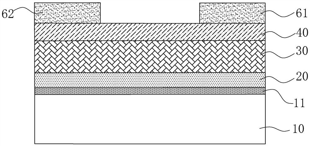
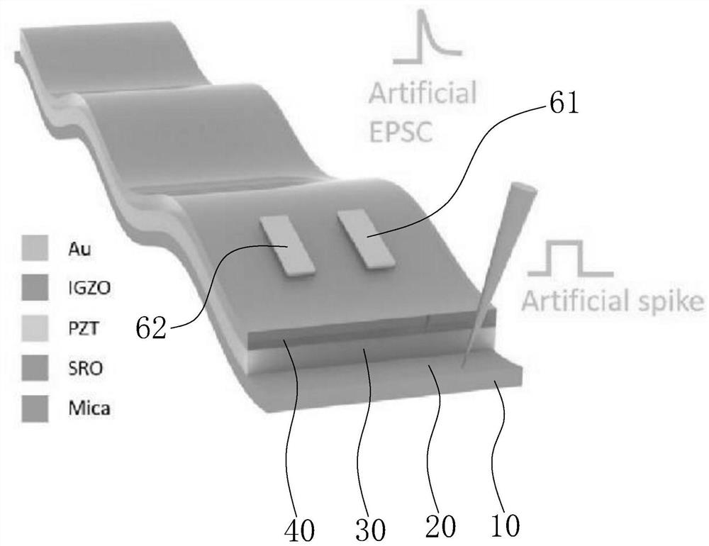
[0064] The following will clearly and completely describe the technical solutions in the embodiments of the present invention with reference to the accompanying drawings in the embodiments of the present invention. Obviously, the described embodiments are only part of the embodiments of the present invention, not all of them. Based on the embodiments of the present invention, other embodiments obtained by persons of ordinary skill in the art on the premise of understanding the inventive concepts of the present invention all fall within the protection scope of the present invention.

[0065] It should be noted that if there is a directional indication (such as up, down, left, right, front, back...) in the embodiment of the present invention, the directional indication is only used to explain the position in a certain posture (as shown in the accompanying drawing). If the specific posture changes, the directional indication will also change accordingly.

[0066] In order to faci...


PUM

PropertyMeasurementUnit
thicknessaaaaaaaaaa
thicknessaaaaaaaaaa
thicknessaaaaaaaaaa

Abstract

The invention relates to an inorganic synaptic transistor structure and a manufacturing method thereof. The structure comprises a flexible substrate; a buffer layer formed on the substrate; a bottom gate electrode formed on the buffer layer; an epitaxial gate dielectric layer formed on the bottom gate electrode; a channel layer formed on the epitaxial gate dielectric layer; and a source electrodeand a drain electrode which are disposed on the channel layer. The manufactured synaptic transistor effectively overcomes the defects that the miniaturization and integration of the synaptic transistor adopting ionic liquid or solid electrolyte as a gate medium are difficult to achieve, the linearity and symmetry of a device are worse, and the synaptic transistor is not resistant to high temperature. The synaptic transistor prepared by the method has flexibility, bending resistance and high temperature resistance, the performance can still be kept basically unchanged under the bending condition or at 100 DEG C, and the energy consumption of each device in the learning process is only 10-30 pJ, which is beneficial to the practical application of the synaptic transistor in the field of high-precision artificial neuromorphic calculation.

Description

technical field [0001] The invention relates to the technical field of a synaptic device simulating a biological synaptic form and its manufacture, in particular to a structure and a manufacturing method of an inorganic synaptic transistor. Background technique [0002] With the rapid development of artificial intelligence, from real-time big data analysis, mechanical automation control to visual and auditory recognition, the demand for various intelligent tasks is exploding globally. At present, it is mainly processed by a computer based on the von Neumann architecture, which requires huge energy consumption and complex algorithms, and it is difficult to break through the relevant bottleneck of data transmission between the memory and the central processing unit (von Neumann bottleneck). Neuromorphic computing simulates the simultaneous processing and storage of data by the human brain, overcomes the von Neumann bottleneck, and can achieve extremely high computing efficienc...

Claims


Application Information

Patent Timeline
Patent Type & Authority Applications(China)
IPC IPC(8): H01L29/423H01L29/51H01L29/78H01L21/34H01L21/44G06N3/063
CPCG06N3/063H01L29/401H01L29/42356H01L29/42364H01L29/516H01L29/66969H01L29/78391
Inventor 钟高阔李江宇訾孟飞唐铭锴黄明强任传来
Owner SHENZHEN INST OF ADVANCED TECH
Why Eureka
Try Eureka