Trench junction barrier schottky structure with enhanced contact area integrated with a mosfet

A metal-oxide half-field and integrated structure technology, applied in the direction of transistors, semiconductor devices, diodes, etc., can solve the problem that the Schottky junction area cannot be effectively reduced, the forward voltage difference of the Schottky diode cannot be effectively reduced, and the components can be reduced. Efficiency etc.

Inactive Publication Date: 2013-01-02
SINOPOWER SEMICON
View PDF4 Cites 5 Cited by
  • Summary
  • Abstract
  • Description
  • Claims
  • Application Information

AI Technical Summary

Problems solved by technology

In the increasingly shrinking trend of component design, the Schottky junction area of ​​the invention cannot be effectively reduced, so that the forward voltage difference of the Schottky diode cannot be effectively reduced, thereby reducing the efficiency of components

Method used


Image

  • Trench junction barrier schottky structure with enhanced contact area integrated with a mosfet
  • Trench junction barrier schottky structure with enhanced contact area integrated with a mosfet
  • Trench junction barrier schottky structure with enhanced contact area integrated with a mosfet

Examples


no. 1 example

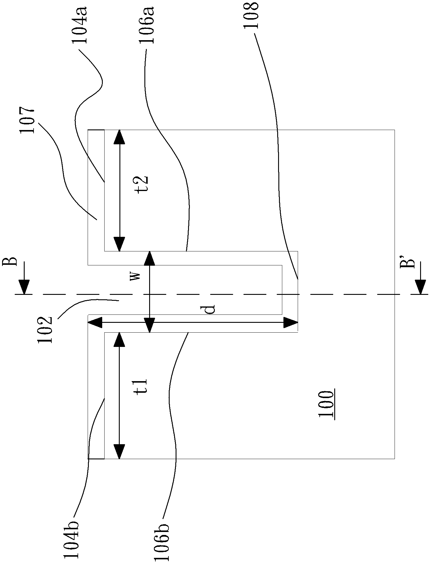
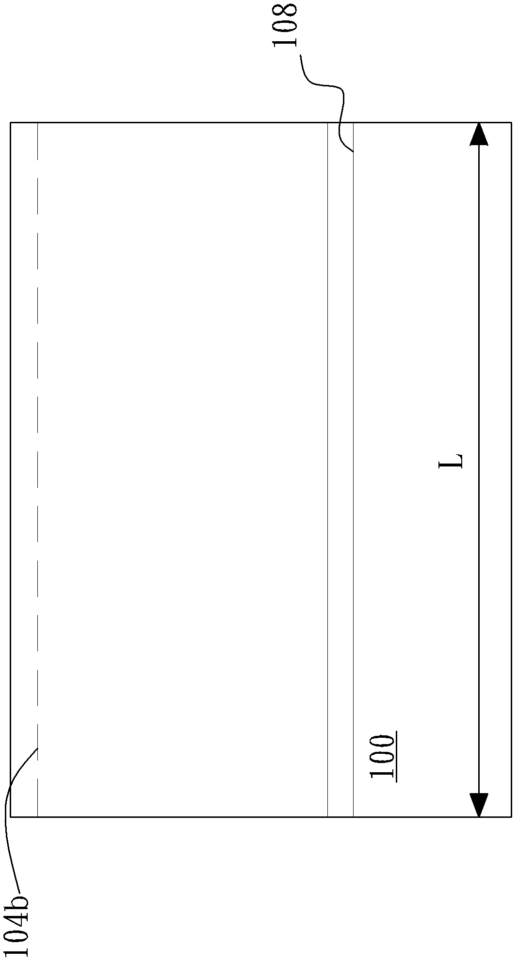
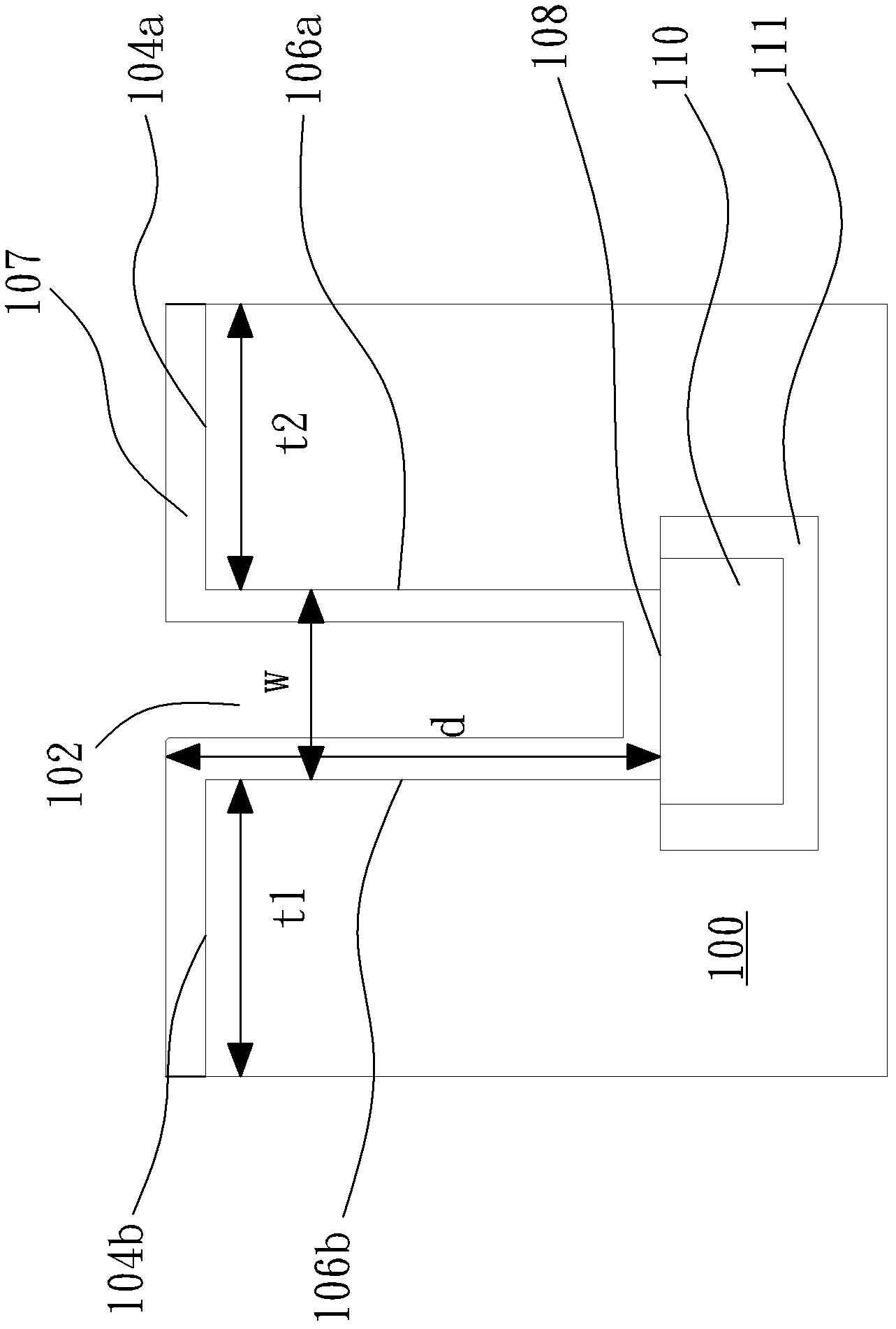
[0023] Figure 1A A sectional view illustrating a Schottky diode of the present invention. An n-type semiconductor substrate 100 is provided with a groove 102, the groove 102 includes a first side wall 106a, a second side wall 106b and a bottom platform 108, the position of the second side wall 106b is relative to the first side wall 106a. The bottom platform 108 is formed at one end of the trench 102 , and a trench opening corresponding to the bottom platform 108 is formed at the other end of the trench 102 . Next to the trench opening, there is an upper platform adjacent to the trench, for example, a first upper platform 104 a adjacent to the right side of the trench 102 and a second upper platform 104 b adjacent to the left side of the trench 102 . The inner surface of the trench 102 is composed of the first side wall 106 a , the second side wall 106 b and the surface of the bottom platform 108 .

[0024] A Schottky barrier metal 107 covers the inner surface of the trench...

no. 2 example

[0044] Please refer to figure 2 , which illustrates a cross-sectional view of a Schottky diode comprising a plurality of trenches and an upper mesa disposed on an n-type semiconductor substrate 200 .

[0045] The trench 202 includes a first side wall 212 a , a second side wall 212 b and a bottom platform 207 . Wherein the first side wall 212a is opposite to the second side wall 212b. An upper platform 214 is adjacent to the trench 202 . A Schottky barrier metal 208 covers the first side wall 212 a , the second side wall 212 b , the bottom platform 207 and the upper platform 214 . A contact metal 204 covers the barrier metal 208 to electrically connect the Schottky diode to external signals. A guard region 210 is located under the bottom platform 207 and doped with a p-type dopant to block the drain flowing under the bottom platform 207 from opposite sides of the first sidewall 212a and the second sidewall 212b. current.

[0046] Please continue to refer to figure 2 , t...

no. 3 example

[0051] Please refer to image 3 , illustrating an integrated structure of a Schottky diode and a MOSFET using a photomask process. The process includes the following steps:

[0052] Step S11: forming a metal oxide semiconductor field effect transistor (MOSFET) in a semiconductor substrate of a first conductivity type, and the metal oxide semiconductor field effect transistor (MOSFET) includes a source electrode;

[0053] Step S12: forming an insulating layer on the semiconductor substrate;

[0054] Step S13: disposing at least one trench and at least one upper platform on the semiconductor substrate of the first conductivity type, and the at least one upper platform is adjacent to the at least one trench;

[0055] Step S14: forming a region under the bottom of the trench, and the region is of a second conductivity type, the second conductivity type being opposite to the first conductivity type;

[0056] Step S15: removing the insulating layer from the at least one upper pla...


PUM


Abstract

An object of this invention is to provide a Schottky diode structure to increase the contact area at a Schottky junction between the Schottky Barrier metal and a semiconductor substrate. The larger contact area of the Schottky junction is, the lower of the forward voltage drop across the Schottky diode will be, thereby improving the performance and efficiency of the Schottky diode. The present invention also discloses that a plurality of trenches with adjacent top mesas can be used to form a Schottky diode with even larger contact area, wherein the trenches are built using the isolation area between two cells of MOSFET with minimum extra overhead by shrinking the dimension of pitch between two trenches.

Description

technical field [0001] The invention relates to a metal oxide half field effect transistor (MOSFET) technology, in particular to a structure of a metal oxide half field effect transistor (MOSFET) integrating a Schottky diode and a manufacturing method for the structure. Background technique [0002] Power converters are often used in a typical pulse width modulation (PWM) circuit, the goal of which is to generate the output voltage of a DC-DC converter, the converter's power high-side metal-oxide-semiconductor field-effect transistor (MOSFET) and the power A low-side MOSFET trims the power of this output voltage. During operation, it usually takes a long time for the power low side (LS) MOSFET to switch from the off state to the on state. During this time period, when the voltage applied to the drain is higher than the voltage of the source, a The built-in diode will be turned on, and a current will pass through the built-in diode through the drain and lead to the power hig...

Claims


Application Information

Patent Timeline
Patent Type & Authority Applications(China)
IPC IPC(8): H01L29/417H01L27/07
CPCH01L29/782H01L29/0623H01L29/417H01L29/66734H01L29/47H01L29/41708H01L27/0629H01L29/41766H01L29/456H01L29/7813H01L29/872H01L27/07H01L29/66727H01L29/1095H01L29/66143
Inventor 戴嵩山李柏贤杨国良廖显皜
Owner SINOPOWER SEMICON
Why Eureka
Try Eureka