Refrigeration structure for three-dimensional encapsulation of micro-electronics and preparation method thereof

A three-dimensional packaging and microelectronics technology, applied in the direction of electric solid device, semiconductor/solid state device manufacturing, circuit, etc., can solve the problems of reducing the reliability of chip operation, increasing the volume of integrated devices, increasing refrigerant exposure, etc. Realize, improve heat dissipation efficiency, and the effect of high process integration

Inactive Publication Date: 2010-03-10
SHANGHAI JIAO TONG UNIV
View PDF0 Cites 8 Cited by
  • Summary
  • Abstract
  • Description
  • Claims
  • Application Information

AI Technical Summary

Problems solved by technology

[0004] The water-cooling channel structure is constructed in an embedded way, so that the water-cooling channel directly acts on the working chip, which reduces the reliability of the chip, and the complex channel structure increases the probability of refrigerant exposure; the water-cooling structure must be considered in the heat dissipation circuit The supply mechanism will inevitably increase the volume of integrated devices; this is contrary to the original intention of reducing the volume of high-integration chips, so for the integration of high-power devices with strict requirements on volume, embedded water cooling is not suitable

Method used


Image

  • Refrigeration structure for three-dimensional encapsulation of micro-electronics and preparation method thereof
  • Refrigeration structure for three-dimensional encapsulation of micro-electronics and preparation method thereof

Examples


Embodiment Construction

[0022] The embodiments of the present invention are described in detail below. This embodiment is implemented on the premise of the technical solution of the present invention, and detailed implementation methods and specific operating procedures are provided, but the protection scope of the present invention is not limited to the following implementation example.

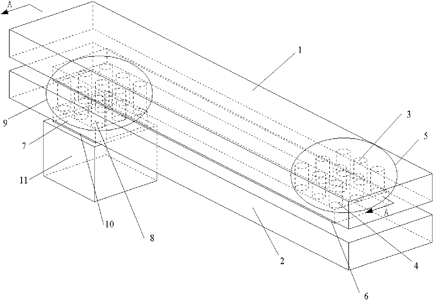
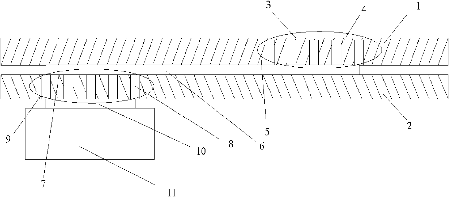
[0023] Such as figure 1 with figure 2 As shown, the refrigeration structure used for microelectronic three-dimensional packaging includes: an upper stacked chip 1 and a lower stacked chip 2, a first vertical metal heat dissipation channel array 5, a second vertical metal heat dissipation channel array 9 and a horizontal metal heat dissipation channel array 6 , wherein: the lower surface of the upper stacked chip 1 and the upper surface of the lower stacked chip 2 are respectively provided with a first vertical metal heat dissipation channel array 5 and a second vertical metal heat dissipation channel array 9, and...


PUM


Abstract

The invention relates to a refrigeration structure for three-dimensional encapsulation of micro-electronics in the micro-electronic encapsulation field and a preparation method thereof. The refrigeration structure comprises two laminated chips, two longitudinal metal heat dissipation passage arrays and a transverse metal heat dissipation passage array, wherein the lower surface of an upper laminated chip and the upper surface of a lower laminated chip are respectively provided with one longitudinal metal heat dissipation passage array; the two longitudinal metal heat dissipation passage arraysare connected by the transverse metal heat dissipation passage array. The preparation method of the invention aiming at heat dissipation passages of local hot spots can selectively adopt metal material with high thermal conductivity as heat dissipation passages on one hand, and can adopt a feasible shortest heat dissipation route aiming at the local hot spots on the other hand, thus increasing the heat dissipation efficiency of the laminated high integration level chip to the largest extent. The invention has high technology integration level and is easy to realize.

Description

technical field [0001] The invention relates to a device in the field of microelectronic packaging and a preparation method thereof, in particular to a refrigeration structure for microelectronic three-dimensional packaging and a preparation method thereof. Background technique [0002] With the high-density development of electronic products driven by Moore's Law, packaging technology is also developing in the direction of high density, miniaturization, multi-chip and three-dimensional scale. In order to reduce the packaging area more efficiently, a three-dimensional stacked package with multiple chips has been developed. structure. The three-dimensional stack package is composed of two or more chips packaged in a single device through electrical interconnection, which can effectively reduce the volume of the device, but it also brings about the heat dissipation problem of high-power devices. [0003] A search of existing literature found (Fabrication of Silicon Carriers w...

Claims


Application Information

Patent Timeline
Patent Type & Authority Applications(China)
IPC IPC(8): H01L25/00H01L23/367H01L21/48
Inventor 丁桂甫王艳孙舒婧
Owner SHANGHAI JIAO TONG UNIV
Why Eureka
Try Eureka