Optical element manufacturing method and optical element

一种光学元件、制造方法的技术,应用在光学元件、光学头制造、光学等方向

Active Publication Date: 2010-03-24
KONICA MINOLTA OPTO
View PDF4 Cites 0 Cited by
  • Summary
  • Abstract
  • Description
  • Claims
  • Application Information

AI Technical Summary

Problems solved by technology

However, optical elements such as beam shaping elements, especially the beam shaping elements used in blue-violet semiconductor lasers are required to have very high shape accuracy, and the method described in Patent Document 3 alone cannot fully cope with it, which is a big problem.

Method used


Image

  • Optical element manufacturing method and optical element
  • Optical element manufacturing method and optical element
  • Optical element manufacturing method and optical element

Examples


Embodiment 1~5

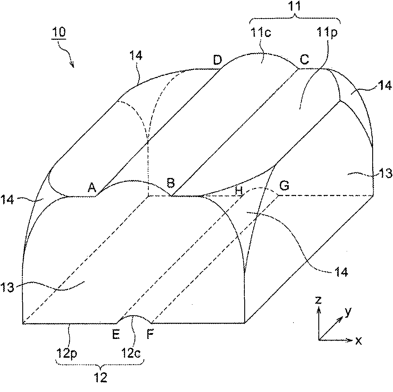
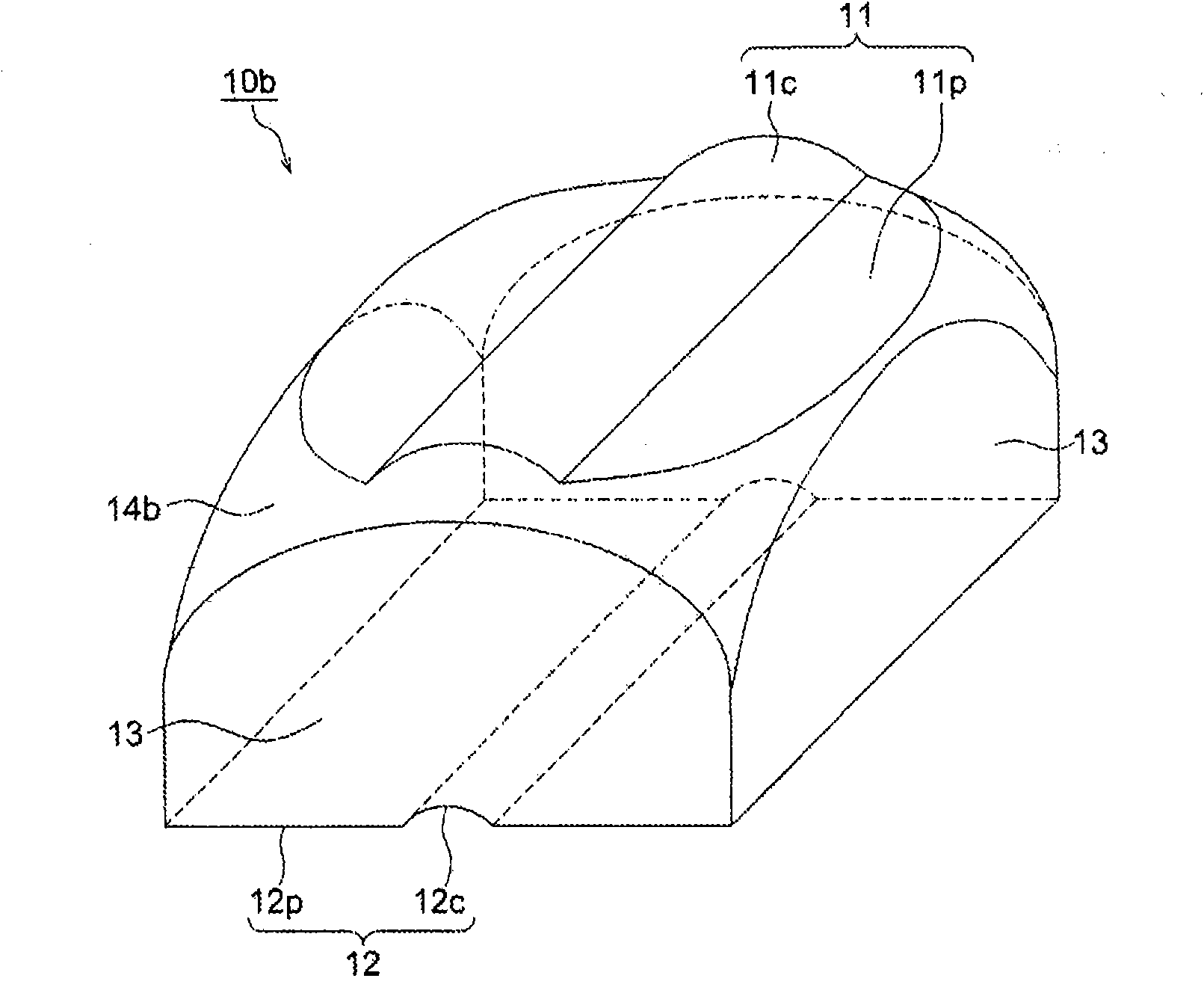
[0101] use Figure 6 The molding die 30 shown produces a figure 1 The optical element 10 is shown. The materials of the upper mold 31, the lower mold 32 and the side mold 33 all adopt superhard materials with tungsten carbide as the main component. The heating temperature of the molding die 30 was 450° C. for the upper die 31 , 470° C. for the lower die 32 , and 470° C. for the side die 33 .

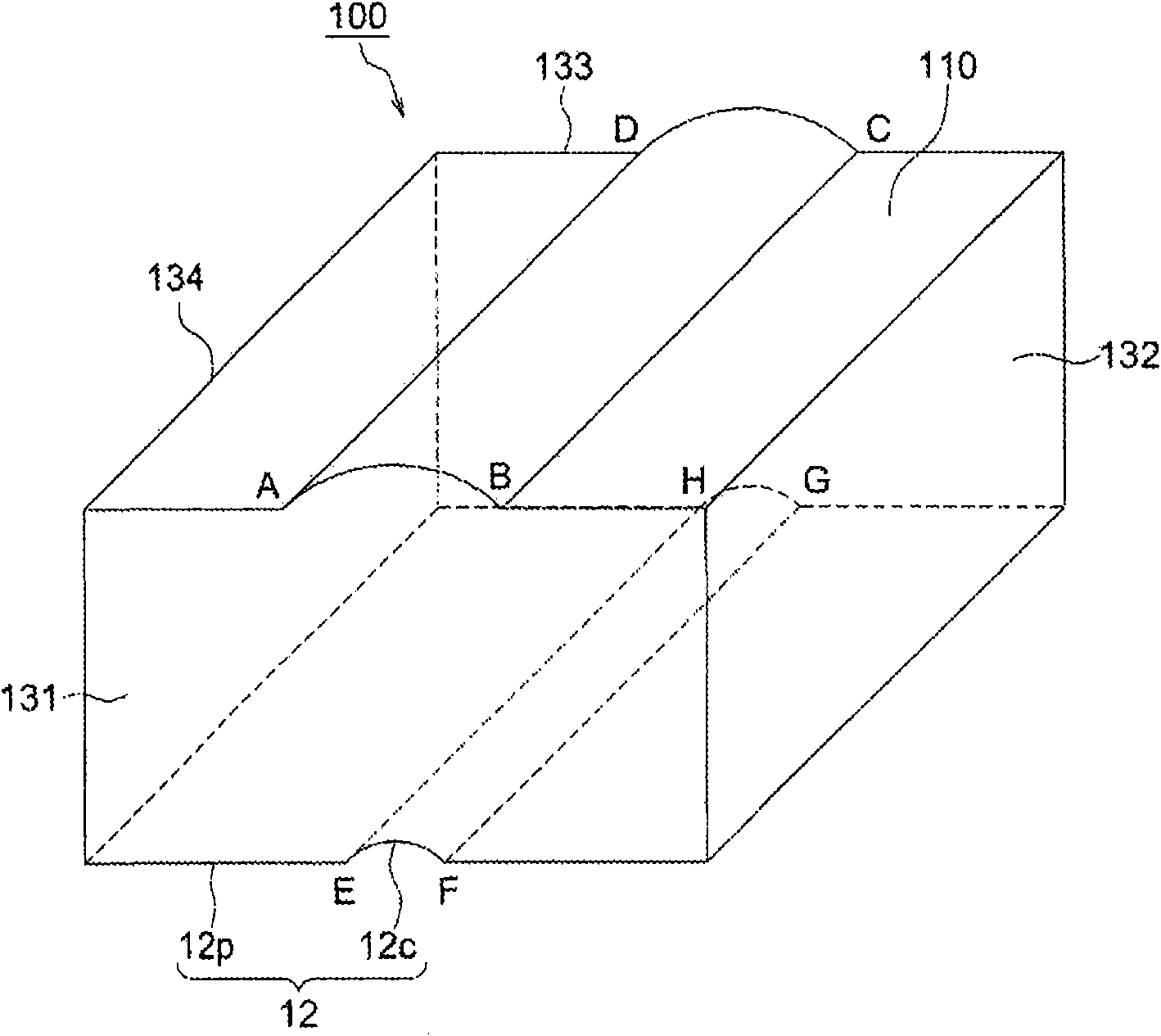
[0102] The optical surface 11c of the optical element 10 is a cylindrical surface, and the section perpendicular to the generatrix is ​​formed by an arc with a radius of 3mm. The optical surface 12c is a cylindrical surface, and the section perpendicular to the generatrix is ​​formed by an arc with a radius of 2mm. The thickness of the central part was made 4 mm. Additionally, make image 3 The shown extended upper forming surface 110 has a circumference of 4 mm x 4 mm, and the extended side forming surface 132 has a height of 4.1 mm. At this moment, the volume of the most filled sp...


PUM


Abstract

Provided is an optical element manufacturing method by which optical elements, such as a beam shaping element having a molded side surface, are highly efficiently and accurately manufactured by pressure-molding a molten glass drop. After supplying a lower molding die with the molten glass drop of a prescribed volume at a temperature higher than that of the molding die, the molten glass drop is pressure-molded by the molding die, and a free surface which is solidified without being in contact with the molding die is formed between a molded upper surface and the molded side surface. The volume of the molten glass drop to be supplied is 0.8 times or more but not more than 0.97 times the volume of a space configured by an extended molded upper surface, an extended molded side surface and the molded lower surface when the molded upper surface and the molded side surface are extended.

Description

technical field [0001] The present invention relates to a manufacturing method of an optical element and an optical element for press-molding molten glass drops to manufacture an optical element, and more particularly, to a manufacturing method of an optical element such as a beam shaping element and an optical element, and the beam shaping element is used for semiconductor The cross-section of the output beam output by the laser is shaped into a circle. Background technique [0002] In an optical pickup device for recording / reproducing information on an optical information recording medium such as a DVD, a semiconductor laser is generally used as a light source. The output beam of the semiconductor laser has an elliptical cross section because it is emitted from the end face of the thin active layer. The elliptical light beam is shaped into a circular light beam by the light beam shaping element before being used, which can improve the utilization efficiency of the light b...

Claims


Application Information

Patent Timeline
Patent Type & Authority Applications(China)
IPC IPC(8): C03B11/00C03B11/08G02B3/00G11B7/135G11B7/22
CPCC03B11/08G02B27/0916G02B3/06G02B27/0966C03B2215/72G02B19/0052G02B19/0014C03B2215/49
Inventor 小椋和幸釜田善浩
Owner KONICA MINOLTA OPTO
Why Eureka
Try Eureka