Package for semiconductor device and packaging method thereof

A semiconductor and flip-chip technology, which is applied in the direction of semiconductor devices, semiconductor/solid-state device manufacturing, semiconductor/solid-state device components, etc., can solve the problems of increasing manufacturing costs, areas where it is difficult to provide relief patterns and intaglio patterns, etc., to achieve Reduce unit production cost, save flux coating process, and improve productivity

Inactive Publication Date: 2010-03-24
OPTOPAC
View PDF0 Cites 13 Cited by
  • Summary
  • Abstract
  • Description
  • Claims
  • Application Information

AI Technical Summary

Problems solved by technology

However, additional processes for forming relief and intaglio patterns increase manufacturing costs
Also, when a high degree of integration is required, it is difficult to provide areas for forming relief patterns and intaglio patterns

Method used


Image

  • Package for semiconductor device and packaging method thereof
  • Package for semiconductor device and packaging method thereof
  • Package for semiconductor device and packaging method thereof

Examples


Embodiment Construction

[0042] Hereinafter, specific embodiments of the present invention will be described in detail with reference to the accompanying drawings.

[0043] This invention may, however, be embodied in different forms and should not be construed as limited to only the embodiments set forth herein. Rather, these embodiments are provided so that this disclosure will be thorough and complete, and will fully convey the scope of the invention to those skilled in the art.

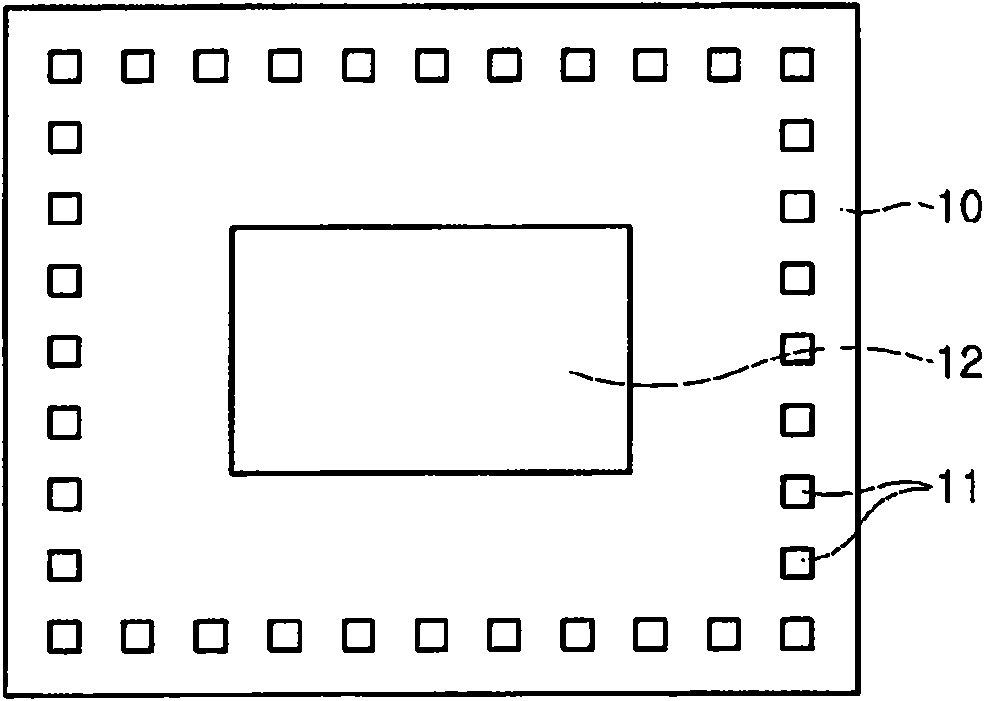
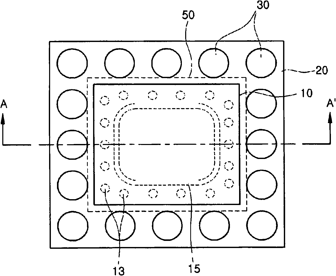
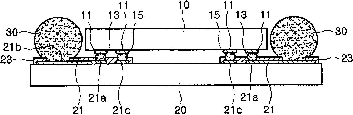
[0044] figure 1 is a schematic plan view of a typical semiconductor device, figure 2 is a schematic plan view of a semiconductor device package according to a first embodiment of the present invention. image 3 and Figure 4 is along figure 2 A schematic cross-sectional view of a semiconductor device package taken along line A-A'.

[0045] As shown in the figure, the semiconductor device package according to the present invention includes a semiconductor device 10 and a substrate 20 disposed opposite to the semicond...


PUM


Abstract

A semiconductor device package and a method thereof are able to reliably package a semiconductor device on a substrate without using flux. The semiconductor device package includes a semiconductor device and a substrate reciprocally disposed with respect to the semiconductor device, wherein the substrate includes a side reciprocal to the semiconductor device on which there are formed a plurality of prominences surrounding an accommodation region where the semiconductor device is to be disposed. The method of packaging a semiconductor device includes preparing the semiconductor device, preparing a substrate, forming a plurality of prominences to surround an accommodation region on the substrate where the semiconductor device is to be disposed, dropping the semiconductor device within the accommodation region, and packaging the semiconductor device on the substrate.

Description

technical field [0001] The present invention relates to a semiconductor device package and a method thereof, which can reliably package a semiconductor device on a substrate without using flux. Background technique [0002] A general semiconductor device (ie, a chip) is usually packaged using a package called a plastic package, in which the semiconductor device is completely sealed with a sealant such as epoxy resin. However, since in the case of an image sensor, in order to sense an image, light must reach an image sensing area on the surface of the image sensor, a general plastic package cannot be utilized. [0003] Therefore, a ceramic package having a cover glass has been widely used as a package of an image sensor. Such ceramic packages are more robust than plastic packages, but require more cost than plastic packages. [0004] Plastic packages and ceramic packages utilize wire bonding to electrically connect bonding pads and terminals of such packages. However, curr...

Claims


Application Information

Patent Timeline
Patent Type & Authority Applications(China)
IPC IPC(8): H01L21/60
CPCH01L2924/1532H01L2924/19105H01L2924/0105H01L2924/01082H01L2224/8191H01L24/29H01L24/73H01L2224/81054H01L2224/81801H01L24/13H01L2224/32014H01L2924/09701H01L2224/16H01L2224/83801H01L2924/19041H01L2924/014H01L2924/01013H01L2224/81191H01L2224/29101H01L2224/8101H01L2924/0665H01L2224/83191H01L2224/2919H01L24/81H01L2224/81211H01L2224/83194H01L2924/01047H01L2224/81136H01L23/49811H01L2924/14H01L24/83H01L2924/01005H01L2924/01033H01L2924/01006H01L2924/01042H01L2924/01058H01L2224/16227H01L2224/16225H01L24/14H01L2224/05568H01L2224/05573H01L2224/06135H01L2224/16237H01L2224/29011H01L2224/29014H01L2224/32237H01L2224/73103H01L2224/73203H01L2924/00011H01L2924/00014H01L2924/1461H01L2924/15788H01L2924/00H01L2224/83205H01L2224/05599H01L23/50H01L27/14
Inventor 金德勋曹永尙李焕哲
Owner OPTOPAC
Why Eureka
Try Eureka