Light emitting diode

一种电极、LED芯片的技术,应用在半导体器件、电气元件、电路等方向,能够解决非均匀电流密度、电流密度高等问题,达到均匀密度的效果

Inactive Publication Date: 2010-03-24
OPTOGAN OY
View PDF0 Cites 6 Cited by
  • Summary
  • Abstract
  • Description
  • Claims
  • Application Information

AI Technical Summary

Problems solved by technology

However, this approach also has its drawbacks: the current density is always highest near the electrodes, especially at the outer ends of the electrode "fingers", resulting in significantly non-uniform current densities

Method used


Image

  • Light emitting diode
  • Light emitting diode
  • Light emitting diode

Examples


Embodiment Construction

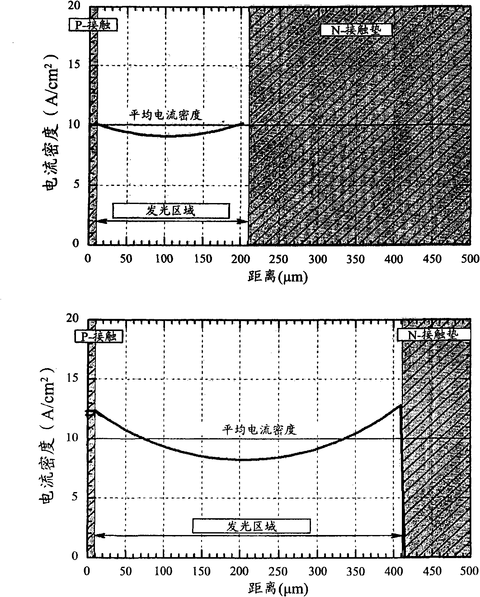
[0019] figure 1 The calculated current densities in linear LED chips with lengths of 200 μm (upper graph) and 400 μm (lower graph) are shown. The current spreading length was 200 μm in both cases. As seen in the figure, the current density is non-uniform in both cases due to the large horizontal dimension relative to the current spreading length, with the uniformity becoming higher with increasing chip length. In the second case it can be seen that the current density is far from uniform.

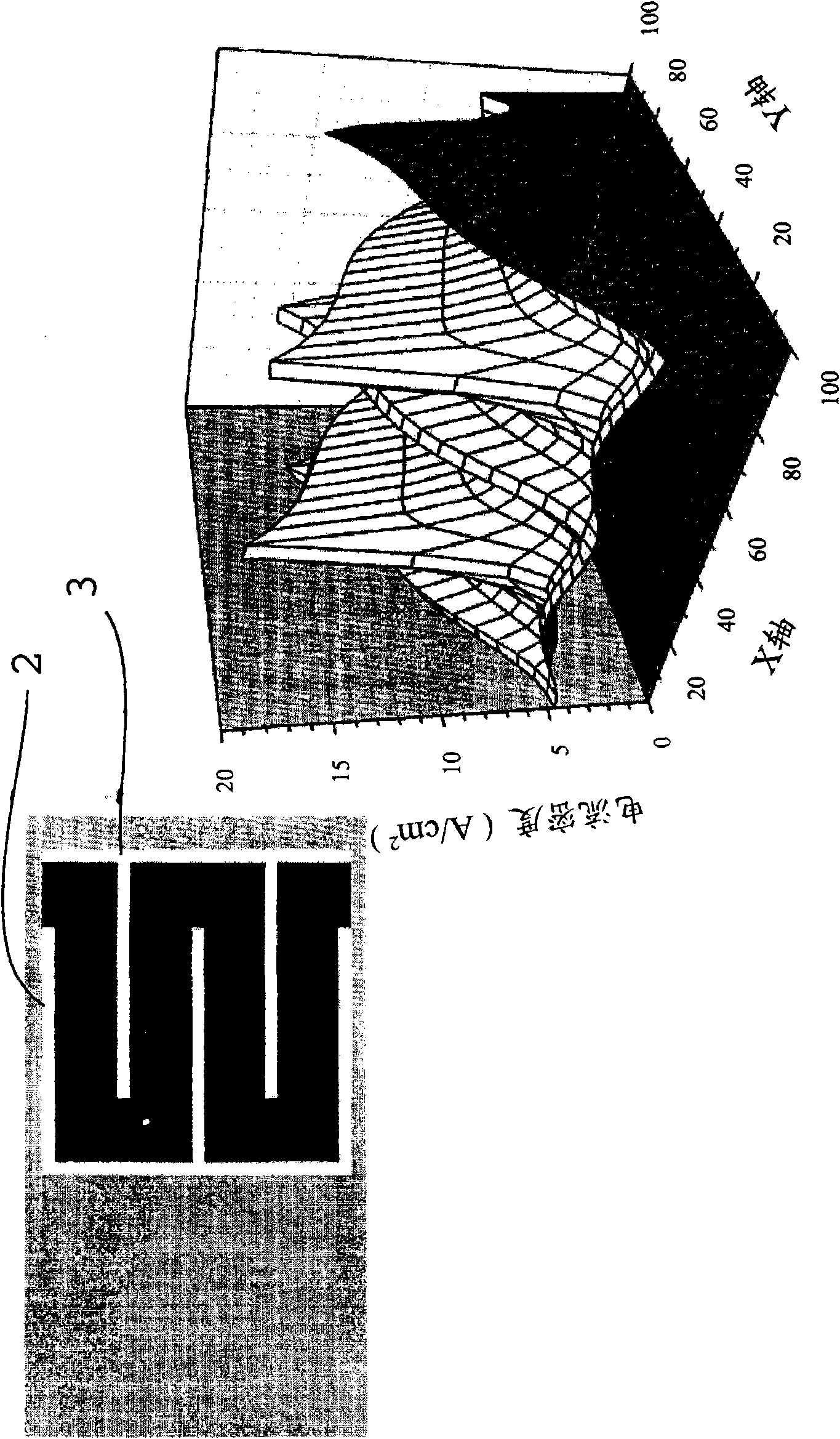
[0020] figure 2 The interdigitated electrodes 2, 3 of the LED design are arranged to provide a distance between electrodes that is less than the current spreading length. Nevertheless, as in figure 2 As seen in the graph of , the current density over the chip area is very inhomogeneous with very strong local maxima at the ends of the electrodes' finger-like protrusions.

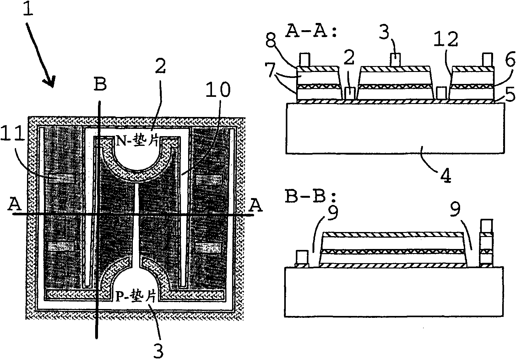
[0021] exist image 3 In the LED chip 1 of , the first electrode 2 and the second electrode 3 establish a modifi...


PUM


Abstract

An LED chip (1) grown on an electrically insulating substrate (4) comprises a lower current-distributing layer (5) of a first conductivity type, a first electrode (2), a vertical layer structure (5, 6, 7), the last two being formed on the lower current- distributing layer horizontally separated from each other, the vertical layer structure comprising an active layer (6) and an upper current-distributing layer (8) of a second conductivity type above the active layer, and a second electrode (3) formed on the upper current-distributing layer, the geometry of the electrodes being adjusted to provide a horizontal distance between the electrodes lower than the current spreading length of the chip. According to the present invention, a vertical trench (9) is formed between the electrodes (2, 3),the trench extending through the chip (1), including the lower current-distributing layer (5), for controlling the horizontal current flow in order to achieve a uniform current density over the activelayer (6).

Description

field of invention [0001] The present invention relates to the design of light emitting diode (LED) chips that are grown on insulating substrates. Background of the invention [0002] In LEDs produced as a layered structure on an insulating substrate, n-contact electrodes and p-contact electrodes are made from the top surface of the chip. They are usually positioned close to opposite edges of the chip's light-generating region. One of them is formed on the lower current distribution layer, which is exposed by selectively etching away the layers grown on it, and the other of them is on the upper current distribution layer on top of the LED layer structure. on the distribution layer. [0003] In a typical case, the horizontal distance between the electrodes is much higher than the total thickness of the vertical layered structure of the LED. In that case, in order to provide high current uniformity over the light generating layers, the sheet resistance of the current distri...

Claims


Application Information

Patent Timeline
Patent Type & Authority Applications(China)
IPC IPC(8): H01L33/00H01L33/20H01L33/38
CPCH01L33/20H01L33/38
Inventor 弗拉德斯拉夫·E·鲍格诺夫马克西姆·A·欧得诺莱多夫
Owner OPTOGAN OY
Why Eureka
Try Eureka