AI technical title is built by Patsnap AI team. It summarizes the technical point description of the patent document.
A phase error and phase difference technology, applied in the system field of reducing phase error, can solve the problems of complex technical solution, not effectively reducing LO phase error, etc., and achieve the effect of simple circuit structure, lower BER, and improved quality
Active Publication Date: 2012-11-21
豪威国际控股有限公司
View PDF1 Cites 0 Cited by
Summary
Abstract
Description
Claims
Application Information
AI Technical Summary
This helps you quickly interpret patents by identifying the three key elements:
Problems solved by technology
Method used
Benefits of technology
Problems solved by technology
[0004] The above technical solution is more complicated, and does not effectively reduce the phase error of LO
Method used
Image
Click on the blue label to locate the original text in one second.
Reading with bidirectional positioning of images and text.
Examples
Embodiment 1
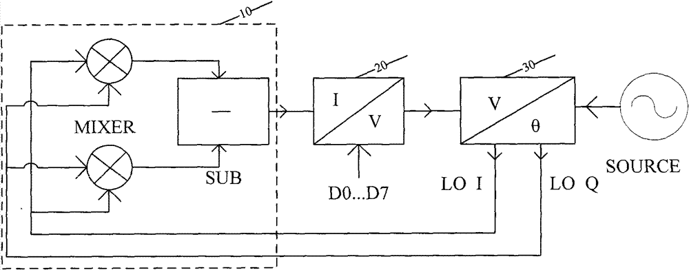
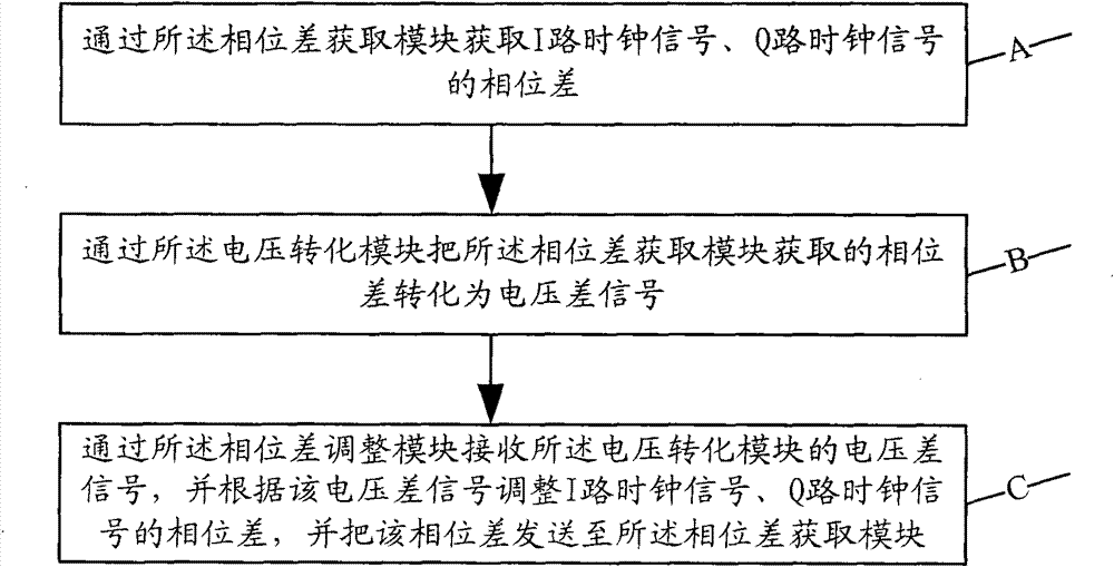
[0033] see figure 1 , figure 2 , the present invention discloses a system for reducing the LO phase error, the system is used to reduce the phase error of the quadrature clock LO, the system includes: a phase difference acquisition module 10 , a voltage conversion module 20 , and a phase difference adjustment module 30 .
[0035] The phase difference obtaining module 10 is used to obtain the phase difference between the I clock signal and the Q clock signal.
[0036] In this embodiment, the phase difference acquisition module includes two mixers and a subtractor, and the two mixers are connected to the subtractor; The clock signals of the two channels are multiplied, and then subtracted by the subtractor to obtain the current information of the phase difference.
[0038] The voltage conversion module 20 is connected with the phase difference acquisition module 10 for converting the phase d...
Embodiment 2
[0049] In this embodiment, the system for reducing the LO phase error includes a phase difference acquisition module, a voltage conversion module, and a phase difference adjustment module.
[0050] exist figure 1 Among them, two multipliers (MIXER, mixer) multiply the clock signal LO I / Q, and after subtraction, wait until the current information of the phase difference is converted into a voltage through I-V, and then adjust the clock through the voltage The phase difference between the I channel and the Q channel of the signal.
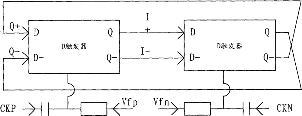
[0051] Such as figure 2 As shown, CKP and CKN are 2 times (or other multiples) of the clock signal of LO, Vfp and Vfn are the voltage difference obtained by phase difference conversion, and the signals I+, I-, Q+, and Q- are the required clock signals . Vfp and Vfn here provide the inverted DC levels of the two D flip-flops, and adjust the phase difference through the different flipping times of the two D flip-flops.
PUM
Abstract
The invention discloses a system and method for reducing LO phase errors. The system comprises a phase difference acquiring module, a voltage transforming module and a phase difference modulating module, wherein the phase difference acquiring module is used for acquiring the phase differences of a I-path clocksignal and a Q-path clocksignal; the voltage transforming module is connected with thephase difference acquiring module and is used for transforming the phase differences acquired by the phase difference acquiring module into voltage difference signals; the phase difference modulatingmodule is used for receiving the voltage difference signals of the voltage transforming module, modulating the phase differences of the I-path clocksignal and the Q-path clock signal through the voltage difference signals and then transmitting the phase differences to the phase difference acquiring module. In the invention, the phase differences of the I-path clock signal and the Q-path clock signal are obtained through two mixers, the phase differences are transformed into voltage, and then the phase errors of the clock signals are adjusted through feedback voltage. The invention can detectand reduce the LO phase errors, reduce bit error rate BER and enhance the communication quality.
Description
technical field [0001] The present invention relates to a system for reducing phase errors, in particular to a system for reducing LO phase errors; in addition, the present invention also relates to a method for realizing the above-mentioned system for reducing LO phase errors. Background technique [0002] In current radio frequency technology, quadrature transmitters and quadrature receivers are used more and more frequently. The use of an orthogonal structure is inseparable from the orthogonal clock (LO). For the transceiver with this structure, the phase error of the LO directly affects its performance. [0003] Later, some research institutions and manufacturers made some attempts to eliminate the phase error of LO. For example, Chinese patent CN200410097121.9 discloses a quadrature signal phase calibrator in the form of a phase-locked loop, which includes a quadrature phase detector, a charge pump, a loop filter, a buffer, a low-pass filter and two controlled delay ...
Claims
Application Information
Patent Timeline
Application Date:The date an application was filed.
Publication Date:The date a patent or application was officially published.
First Publication Date:The earliest publication date of a patent with the same application number.
Issue Date:Publication date of the patent grant document.
PCT Entry Date:The Entry date of PCT National Phase.
Estimated Expiry Date:The statutory expiry date of a patent right according to the Patent Law, and it is the longest term of protection that the patent right can achieve without the termination of the patent right due to other reasons(Term extension factor has been taken into account ).
Invalid Date:Actual expiry date is based on effective date or publication date of legal transaction data of invalid patent.

