Method for increasing breakdown voltage of power MOS field effect transistor

A field effect tube and breakdown voltage technology, which is applied in the manufacture of circuits, electrical components, semiconductors/solid-state devices, etc., can solve the problems of MOS field effects being easily broken down, eliminate angles, increase breakdown voltage, and reduce The effect of electric field strength

Active Publication Date: 2010-05-12
SHANGHAI HUAHONG GRACE SEMICON MFG CORP
View PDF0 Cites 1 Cited by
  • Summary
  • Abstract
  • Description
  • Claims
  • Application Information

AI Technical Summary

Problems solved by technology

[0005] In order to solve the problem in the prior art that the MOS field effect is easily broken down due to the included angle of polysilicon in the MOS field effect, the present invention provides a method for increasing the breakdown voltage of the MOS field effect

Method used


Image

  • Method for increasing breakdown voltage of power MOS field effect transistor
  • Method for increasing breakdown voltage of power MOS field effect transistor
  • Method for increasing breakdown voltage of power MOS field effect transistor

Examples


Embodiment Construction

[0018] The present invention will be further described below in conjunction with the accompanying drawings.

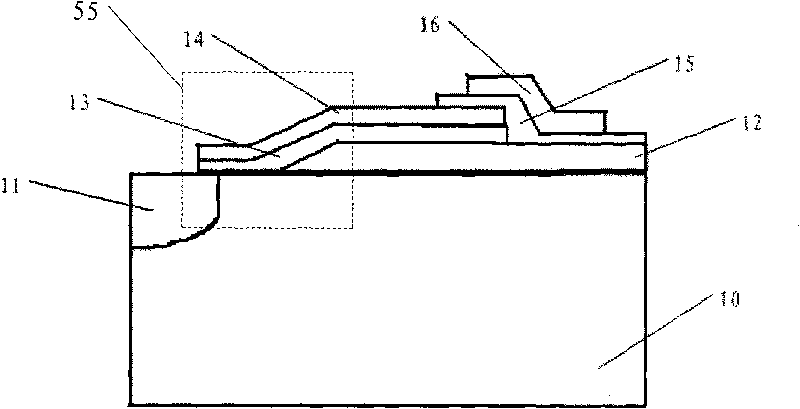
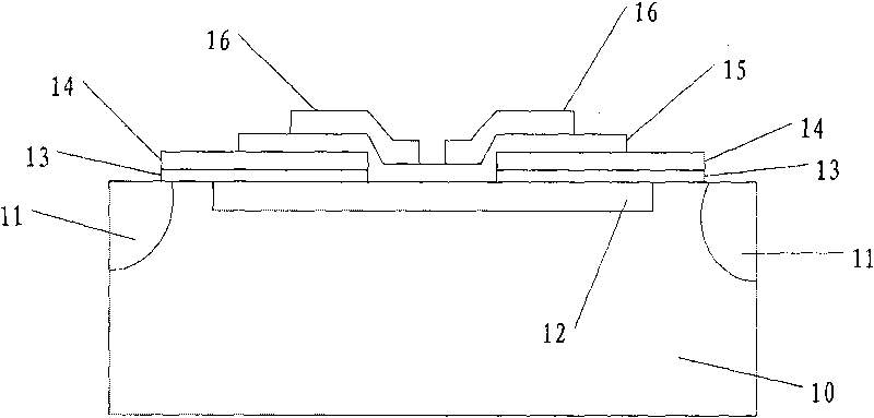
[0019] Because in the field plate of the power MOS field effect transistor in the prior art, there is an included angle formed by a polysilicon layer, the existence of the included angle will attract more electric fields to gather, increase the electric field intensity at the included angle, and make the power MOS Field effect transistors are easily broken down. In order to solve this problem, the present invention proposes a method for improving the breakdown voltage of power MOS field effect transistors. Please refer to figure 2 , it can be seen from the figure that the first oxide layer 12 is completely located in the substrate 10, two active regions 11 are located in the substrate 10 on both sides of the first oxide layer 12, and two polysilicon gates are formed on the substrate 10 and the first oxide layer 12, the second oxide layer 15 is deposited on the polysil...


PUM


Abstract

The invention provides a method for increasing breakdown voltage of a power MOS field effect transistor, comprising the following steps: etching out a first shallow groove in the substrate of the power MOS field effect transistor; depositing a first oxide layer in the first shallow groove; etching out a plurality of second shallow grooves in the first oxide layer; forming two polysilicon gates on the substrate and the first oxide layer; carrying out ion implantation on the surface of the substrate on the outer sides of the two polysilicon gates, thereby forming a first active region and a second active region; depositing a second oxide layer on the polysilicon gate; and fabricating a field plate on the second oxide layer. The method not only eliminates the included angle formed during the growth process of the polysilicon in the power MOS field effect transistor, but also disperses the electric field strength on the surface of the power MOS field effect transistor, thereby reducing the electric field strength on the surface of the power MOS field effect transistor to the utmost extent and increasing the breakdown voltage of power MOS field effect transistor.

Description

technical field [0001] The invention relates to the field of semiconductor manufacturing, in particular to a method for increasing the breakdown voltage of a power MOS field effect transistor. Background technique [0002] Power MOS field effect transistors have been used for many years, and their design and manufacturing methods have been continuously improved. The full name of MOS in English is Metal-Oxide-Semiconductor, that is, metal-oxide-semiconductor. To be precise, this name describes the structure of power MOS field effect transistors in integrated circuits, that is, on semiconductor devices with a certain structure, plus silicon and metal. Structurally speaking, MOS tubes can be divided into enhancement type (E type) and depletion type (D type). Power MOS field effect tubes generally have three electrodes: source (source), drain (drain) and The gate (gate) and the circuit formed by the power MOS field effect transistor are generally called MOS circuits, but there...

Claims


Application Information

Patent Timeline
Patent Type & Authority Applications(China)
IPC IPC(8): H01L21/336H01L21/28
Inventor 吴小利许丹
Owner SHANGHAI HUAHONG GRACE SEMICON MFG CORP
Why Eureka
Try Eureka