Method for manufacturing solar cell

A solar cell and manufacturing method technology, applied in circuits, electrical components, final product manufacturing, etc., can solve the problems of silicon wafer pattern deformation, unusable use, poor pattern accuracy, etc., to reduce losses, improve photoelectric conversion efficiency, The effect of fill factor improvement

Inactive Publication Date: 2011-05-18
JIANGSU SHUNFENG PHOTOVOLTAIC TECH CO LTD
View PDF0 Cites 2 Cited by
  • Summary
  • Abstract
  • Description
  • Claims
  • Application Information

AI Technical Summary

Problems solved by technology

The material of the screen printing screen plate is the screen and the photosensitive adhesive layer, which will not only cause a certain deformation of the graphics during exposure and development, but also cause a certain amount of deformation during printing. Finally, the result obtained on the silicon wafer poor graphics accuracy
Moreover, as the number of printings increases, the screen becomes loose, and the resulting deformation continues to increase, which eventually leads to serious graphics deformation on the silicon wafer, making it impossible to continue to use

Method used


Image

  • Method for manufacturing solar cell
  • Method for manufacturing solar cell
  • Method for manufacturing solar cell

Examples


Embodiment Construction

[0022] The structure and manufacturing method of the solar cell embodiment of the present invention will be described below with reference to the accompanying drawings.

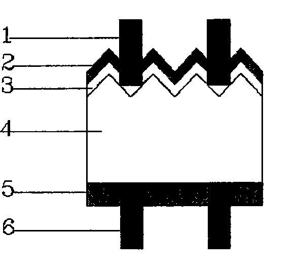
[0023] figure 1 Schematic diagram of the cross-sectional structure of a solar cell. In the figure, the front electrode 1 is the negative electrode, which draws the current on the front of the battery; the anti-reflection film 2 is used to reduce the reflectivity of the battery surface for light; the N-type layer 3 forms a built-in space electric field on the P-type silicon interface to realize the electron and hole drift to achieve the dynamic balance of diffusion carriers; the P-type silicon crystal 4 with texture on the surface is the matrix material of solar cells, and the texture on the surface can reduce the reflectivity of the battery surface for light; the back aluminum layer 5 and P The type silicon substrate 4 realizes ohmic contact and collects carriers on the back surface; the back electrode 6 is ...


PUM

PropertyMeasurementUnit
electrical resistivityaaaaaaaaaa
thicknessaaaaaaaaaa

Abstract

The invention relates to a method for manufacturing a solar cell. The method comprises the following steps of: etching a longitudinal main grating groove and a transverse grating groove on the front surface of a silicon chip by laser, making the surface reacted by adding dilute solution of NaOH to form a pile surface, washing the pile surface by adding dilute solution of HCl and dilute solution of HF in sequence, filling gaseous POCl3 at a temperature of between 850 and 920 DEG C, and performing high-temperature dispersion to form a PN junction on the front surface of the cell; filling SiH4 gas and NH3 gas, forming a surface antireflecting film by the chemical vapor deposition, pre-fabricating a nickel alloy mask plate which is provided with grating-shaped holes corresponding to grating-shaped electrode grooves of the silicon chip, making the grating-shaped holes of the mask plate and the grating-shaped electrode grooves justify, and by using printing equipment, pressing silver paste on the front surface in the grating-shaped electrode grooves on the surface of the silicon chip through the grating-shaped holes in a printing mode; and printing an aluminum layer and the silver paste on the back surface, and in a sintering furnace, sintering the aluminum layer and the silver paste at a temperature of between 850 and 950 DEG C by infrared rays to form electrodes. For the solar cell manufactured by the method, the metal is fully contacted wit the silicon chip, and the photoelectric conversion efficiency is high.

Description

technical field [0001] The invention relates to a method for manufacturing a solar cell. Background technique [0002] With the rapid development of the economy, the sharp increase in energy consumption, and the decreasing reserves of coal and oil, people urgently need to develop the application fields of solar energy. Solar cells are products that convert solar energy into electrical energy developed in recent years. Solar cells are widely used. At present, they are mainly used for domestic electricity in plateaus, islands, pastoral areas, frontier posts and other remote areas without electricity, as well as transportation and communication / communication, petroleum, marine , Meteorology and other fields, unattended microwave relay stations, optical cable maintenance stations, broadcast / communication / paging power systems for outdoor or field various lighting and facilities and equipment. It is also possible to establish 10KW-50MW independent photovoltaic power stations, win...

Claims


Application Information

Patent Timeline
Patent Type & Authority Patents(China)
IPC IPC(8): H01L31/18
CPCY02P70/50
Inventor 潘猛吕达童彩霞黄耀辉瞿辉
Owner JIANGSU SHUNFENG PHOTOVOLTAIC TECH CO LTD
Why Eureka
Try Eureka