Organic light emitting diodde desplay device

一种发光二极管、显示器件的技术,应用在二极管、电固体器件、半导体器件等方向,能够解决色彩稳定性低、蓝色光发光层使用寿命短、大规模生产可行性降低等问题

Active Publication Date: 2010-05-26
LG DISPLAY CO LTD
View PDF1 Cites 9 Cited by
  • Summary
  • Abstract
  • Description
  • Claims
  • Application Information

AI Technical Summary

Problems solved by technology

However, the white light OLED with this stacked structure has the problems of short service life of the blue light-emitting layer, and thus low color stability due to the short service life, and the problem of relatively high driving voltage.
To overcome these problems, the number of layers mentioned above may be increased and the structure may become more complex, resulting in less feasibility for mass production

Method used


Image

  • Organic light emitting diodde desplay device
  • Organic light emitting diodde desplay device
  • Organic light emitting diodde desplay device

Examples


Embodiment Construction

[0024] Below, refer to Figure 1-11 Exemplary embodiments are described.

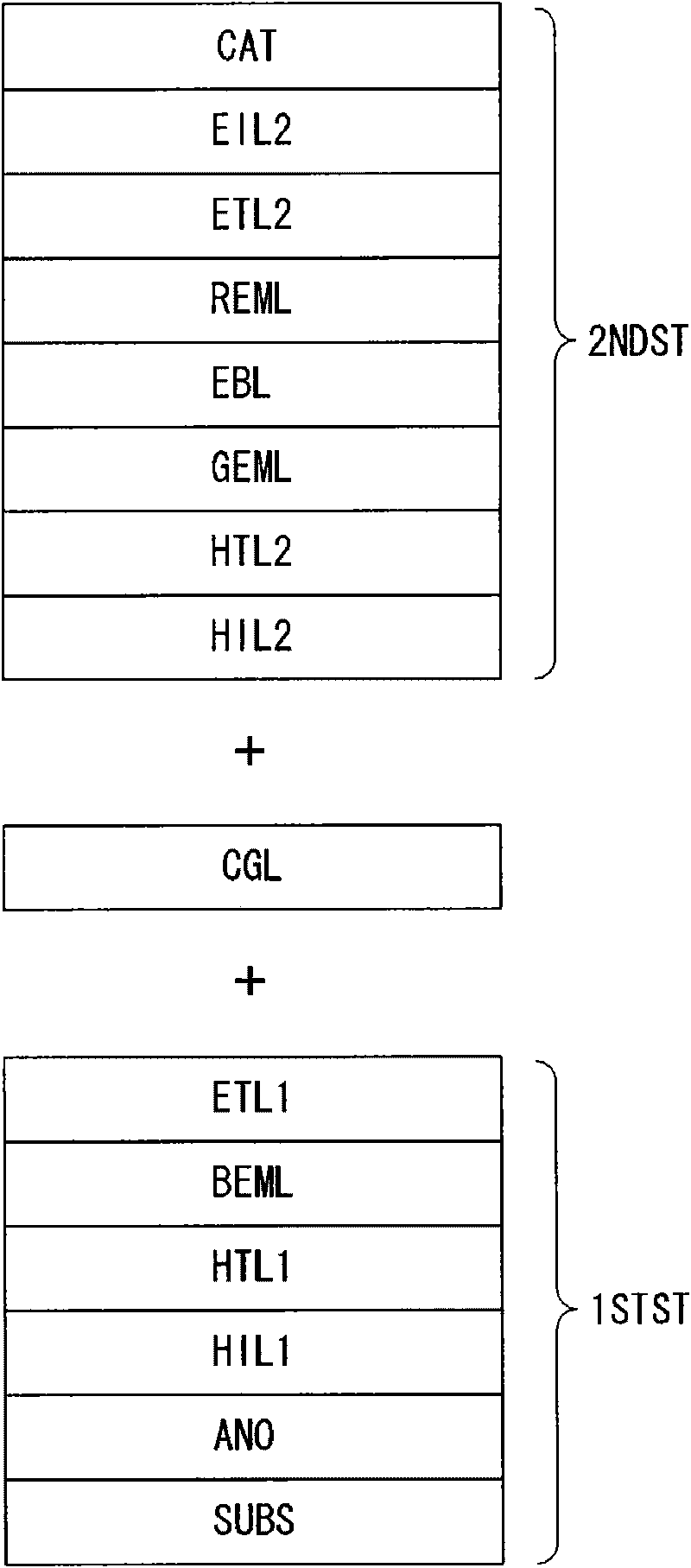
[0025] refer to figure 1 , the OLED display device according to the first exemplary embodiment includes a white OLED emitting white light including red, green, and blue wavelengths.

[0026] The white OLED has the following structure: a cathode CAT; an anode ANO; and first and second stacks between the cathode CAT and the anode ANO. The first stack 1STST emits fluorescence at a blue wavelength. The second stack 2NDST is stacked on the first stack 1STST, and emits fluorescence at a green wavelength and phosphorescence at a red wavelength.

[0027] A charge generation layer (CGL) is formed between the first and second stacks 1STST and 2NDST. The CGL is a material with low optical properties and electrical loss properties, and the material may include, for example, metals, oxides, organics or stacked layers thereof.

[0028] The first stack 1STST includes an anode ANO stacked on the substrate SUBS; a ...


PUM


Abstract

The OLED display device includes a first stack and a second stack that are separated from each other between an anode electrode and a cathode electrode, with a charge generation layer sandwiched between the first stack and the second stack, each of the first stack and the second stack having an emission layer. The first stack includes a blue emission layer formed between the anode electrode and the CGL. The second stack includes a fluorescent green emission layer and a phosphorescent red emission layer formed between the cathode electrode and the CGL. The blue emission layer includes one of afluorescent blue emission layer and a phosphorescent blue emission layer.

Description

[0001] This application claims priority from Korean Patent Application No. 10-2008-0095967 filed September 30, 2008, which is hereby incorporated by reference in its entirety. technical field [0002] The invention discloses an organic light emitting diode display device, which can improve color stability and ensure long service life. Background technique [0003] Recently, various types of flat panel display devices have been developed in order to reduce the weight and volume of the display devices, which are disadvantageous for cathode ray tubes. These flat panel display devices include liquid crystal displays (LCDs), field emission displays (FEDs), plasma display panels (PDPs), and electroluminescent devices (ELs). [0004] An organic light-emitting diode (hereinafter referred to as "OLED") or an electroluminescent device (EL) may include an anode, a cathode, and an organic light-emitting material layer between the anode and the cathode, wherein the anode is generally mad...

Claims


Application Information

Patent Timeline
Patent Type & Authority Applications(China)
IPC IPC(8): H01L51/50H01L51/52
CPCH01L51/5036H01L51/006H01L51/0055H01L27/3209H01L51/0069H01L51/5278H01L51/0058H10K59/32H10K85/623H10K85/626H10K85/633H10K85/656H10K50/125H10K50/19H10K50/15H10K50/16H10K50/17
Inventor 皮性勋
Owner LG DISPLAY CO LTD
Why Eureka
Try Eureka