
Highly luminescent cadmium-free nanocrystals with blue emission

a nanocrystal and blue emission technology, applied in the field of nanotechnology, can solve the problems of limiting the future application of cadmium-based nanoparticles, cadmium, mercury, lead, etc., and achieve the effect of only producing red and green luminescence in the nanostructur

Inactive Publication Date: 2017-03-09
NANOSYS INC
View PDF2 Cites 23 Cited by
  • Summary
  • Abstract
  • Description
  • Claims
  • Application Information

AI Technical Summary

Benefits of technology

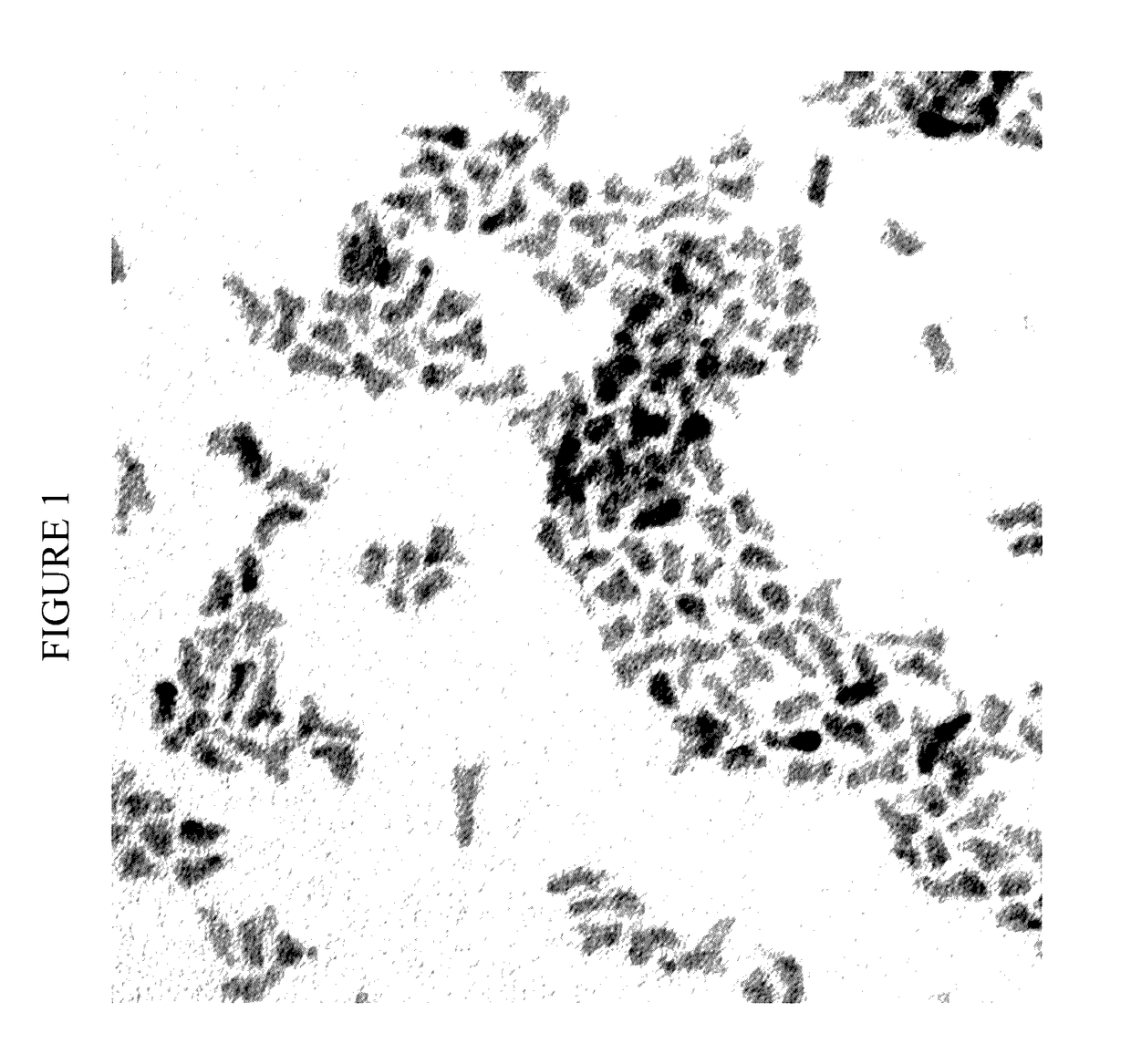
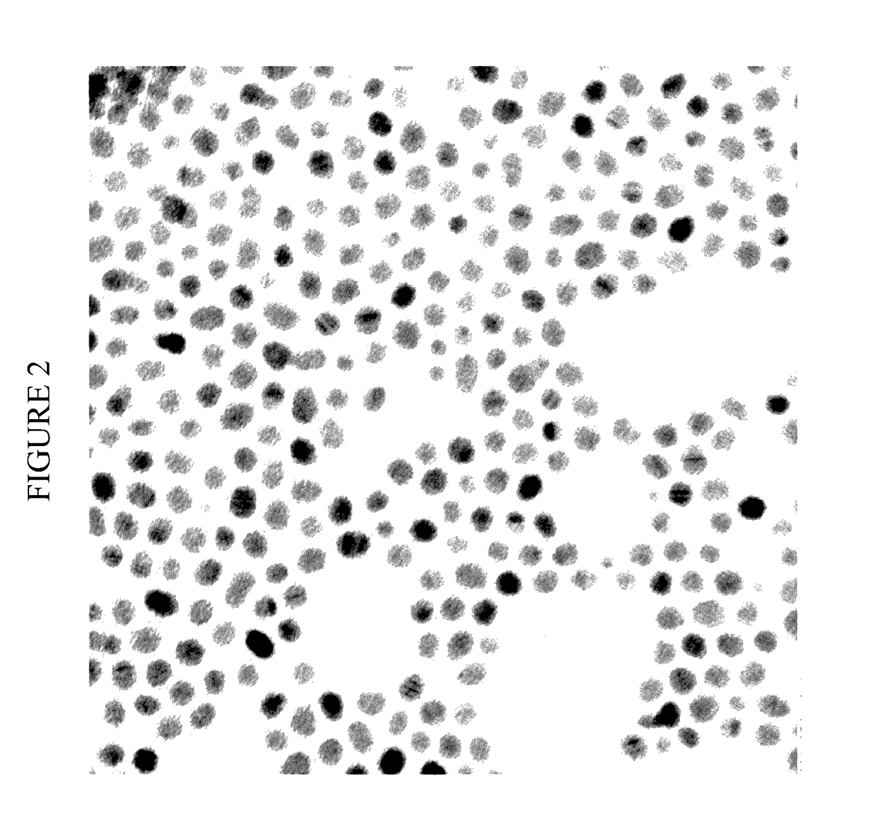
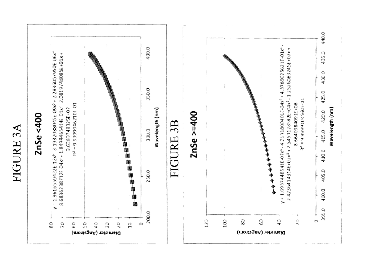
The present invention provides a method of producing a multi-layered nanostructure with a core and shell made of zinc selenium and zinc selenide. The nanostructure has a unique emission wavelength between 400 nm and 460 nm and a high quantum yield. The nanostructure has a particle size between 5 nm and 10 nm and can be embedded in a matrix. The method involves combining a zinc source and a selenium source to produce a reaction mixture, which is then contacted with a solution containing a zinc source and a selenium source. The nanostructure can be produced with a single zinc source and a single selenium source or with a combination of zinc and selenium sources. The method can be repeated to create a multi-layered nanostructure with a different combination of zinc and selenium sources. The nanostructure has potential applications in quantum dots, light-emitting diodes, and biological imaging.

Problems solved by technology

But, there are increasing concerns that toxic materials such as cadmium, mercury, or lead would pose serious threats to human health and the environment and the European Union's Restriction of Hazardous Substances rules ban any consumer electronics containing more than trace amounts of these materials.
CdSe-based nanostructures with high quantum yield and a broad emission spanning the entire visible spectral region have been produced; however, the intrinsic toxicity of cadmium raises environmental concerns which limit the future application of such cadmium-based nanoparticles.
InP-based nanostructures are the best-known substitute for CdSe-based materials; however, due to their relatively small bandgap, In—P based nanostructures can only produce red and green luminescence.
In addition, high quantum yield InP nanostructures have been difficult to obtain.

Method used


Image

  • Highly luminescent cadmium-free nanocrystals with blue emission
  • Highly luminescent cadmium-free nanocrystals with blue emission
  • Highly luminescent cadmium-free nanocrystals with blue emission

Examples


example 1

Synthesis of ZnSe Nanostructures

[0184]For preparation of 9.82 g of ZnSe core (assuming 100% production yield):

[0185]Chemicals used:[0186]Diethylzinc (ZnEt2);[0187]Selenium (Se);[0188]Trioctylphosphine (TOP);[0189]Diphenylphosphine (DPP);[0190]Oleylamine (OYA);[0191]Toluene;[0192]Ethanol (EtOH); and[0193]Hexanes.

[0194]Measure out 15 mL of OYA into a 250 mL 3-neck flask along with a stir bar. Equip the flask with an air-free adaptor on a Schlenk line. Use rubber septa to close the two side-necks of the flask. Evacuate the flask and then purge it with nitrogen. Repeat this step 3 times. Heat the solution to 110° C. and maintain at this temperature for 30 minutes under evacuation.

[0195]Prepare a syringe containing the following chemicals in the glovebox:[0196]DPP / TOP (45% DPP by weight)—500 μL;[0197]TOP—1 mL; and

[0198]HSe—1.5 mL (1.92 M solution of Se dissolved in TOP).

[0199]Prepare an injection solution containing the following chemicals in the glovebox:[0200]TOP—2.5 mL; and[0201]ZnEt2...


PUM

PropertyMeasurementUnit
emission wavelengthaaaaaaaaaa
particle sizeaaaaaaaaaa

Abstract

Highly luminescent nanostructures comprising a ZnSe core and ZnS shell layers, particularly highly luminescent quantum dots, are provided. The nanostructures have high photoluminescence quantum yields and in certain embodiments emit light at particular wavelengths and have a narrow size distribution. Processes for producing such highly luminescent nanostructures and techniques for shell synthesis are also provided.

Description

CROSS-REFERENCE TO RELATED APPLICATION[0001]This application claims priority benefit of U.S. Provisional Application No. 62 / 216,093, filed Sep. 9, 2015, which is hereby incorporated by reference in its entirety.BACKGROUND OF THE INVENTION[0002]Field of the Invention[0003]The invention pertains to the field of nanotechnology. More particularly, the invention relates to highly luminescent nanostructures, particularly highly luminescent nanostructures comprising a ZnSe core and ZnS shell layers. The invention also relates to methods of producing such nanostructures.[0004]Background Art[0005]Semiconductor nanostructures can be incorporated into a variety of electronic and optical devices. The electrical and optical properties of such nanostructures vary, e.g., depending on their composition, shape, and size. For example, size-tunable properties of semiconductor nanoparticles are of great interest for applications such as light emitting diodes (LEDs), lasers, and biomedical labeling. Hig...

Claims


Application Information

Patent Timeline
Patent Type & Authority Applications(United States)
IPC IPC(8): C09K11/88C09K11/02C09K11/56
CPCC09K11/883C09K11/565C09K11/025B82Y40/00Y10S977/95Y10S977/774Y10S977/892Y10S977/896B82Y20/00C09K11/02
Inventor TRUSKIER, JONATHANKAN, SHIHAI
Owner NANOSYS INC
Learn More