Organic electroluminescent white light device with multi-luminescent layer

A white light device and organic light-emitting layer technology, applied in the field of organic electroluminescent devices, can solve the problems of poor anthracene film formation, high voltage, easy breakdown, etc., and achieve the effects of improving efficiency, performance, and device brightness.

Inactive Publication Date: 2007-08-22
JILIN UNIV
View PDF1 Cites 20 Cited by
  • Summary
  • Abstract
  • Description
  • Claims
  • Application Information

AI Technical Summary

Problems solved by technology

In 1982, Vincet et al. made a 50nm-thick anthracene film by vacuum evaporation, and observed blue fluorescence when the voltage was further lowered to 30V, but its external quantum efficiency was only about 0.03%, which was mainly because the electron injection efficiency was too high. Low and anthracene's poor film-forming properties and easy breakdown; in 1983, Partridge published an article on polymer electroluminescence, but due to the low brightness obtained, his work did not attract widespread attention
In short, in the mid-1960s and 1980s, OLED hovered at the level of high voltage, low brightness, and low efficiency.

Method used


Image

  • Organic electroluminescent white light device with multi-luminescent layer
  • Organic electroluminescent white light device with multi-luminescent layer
  • Organic electroluminescent white light device with multi-luminescent layer

Examples


Embodiment 1

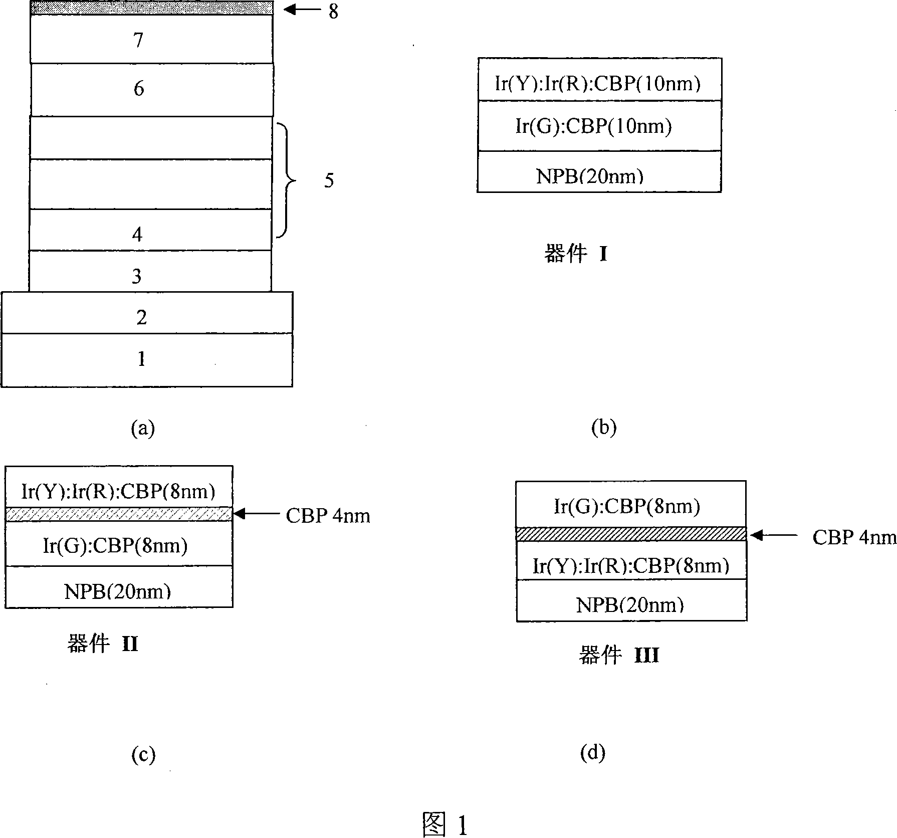
[0038] (1) To transparent conductive substrate ITO glass, carry out acetone, ethanol, deionized water to scrub successively, then carry out acetone, ethanol, deionized water ultrasonic cleaning to it again successively, carry out ultraviolet ozone treatment to it after drying;

[0039] (2) Place the above-mentioned pretreated ITO glass in the vacuum chamber of the evaporation equipment, and evacuate to 3×10 -4 Within Pa, evaporate 30nm m-MTDATA on the ITO film as a hole injection layer, and the evaporation rate is 0.1-0.2nm / s;

[0040] (3) Keeping the pressure in the above vacuum chamber constant, first evaporate a 20nm NPB layer as a hole transport layer and a blue light-emitting layer, and then evaporate a 10nm doped Ir(ppy) layer 3 A CBP layer with a concentration of 8wt% is used as a green light-emitting layer; finally, 10nm is evaporated and doped with 5wt% (F-BT) 2 Ir(acac) and 3wt% Ir(piq) 2 The CBP layer of acac is used as the yellow and red light-emitting layers;

...

Embodiment 2

[0046] (1) with embodiment 1;

[0047] (2) with embodiment 1;

[0048] (3) Keep the pressure in the above vacuum chamber constant, first evaporate a 20nm NPB layer as a hole transport layer and a blue light-emitting layer; sequentially evaporate 8nm doped Ir(ppy) 3 The CBP layer with a concentration of 8wt% is used as the green light-emitting layer; a 4nm non-doped CBP layer is evaporated to block the triplet energy transfer from the green dye to the yellow and red dyes; 5wt% (F-BT) 2 Ir(acac) and 3wt%Ir(piq) 2 The CBP layer of acac is used as the yellow light and red light emitting layers. The evaporation speed of these two layers is the same as that in Example 1, and the evaporation time is 40-80s;

[0049] (4) with embodiment 1;

[0050] (5) with embodiment 1;

[0051] (6) Same as in Example 1, to prepare device II.

Embodiment 3

[0053] (1) with embodiment 1;

[0054] (2) with embodiment 1;

[0055] (3) Keep the pressure in the above-mentioned vacuum chamber constant, first evaporate a 20nm NPB layer as a hole transport layer and a blue light-emitting layer; 2 Ir(acac) and 3 wt% Ir(piq) 2 The CBP layer of acac is used as the yellow and red light-emitting layer; then a 4nm non-doped CBP layer is evaporated to block the triplet energy transfer from the green dye to the yellow and red dyes; finally, the 8nm doped layer is evaporated Ir(ppy) 3 Concentration is the CBP layer of 8wt% as green light-emitting layer, and evaporation speed and evaporation time are the same as embodiment 2;

[0056] (4) with embodiment 1;

[0057] (5) with embodiment 1;

[0058] (6) Same as Example 1, prepare device III.

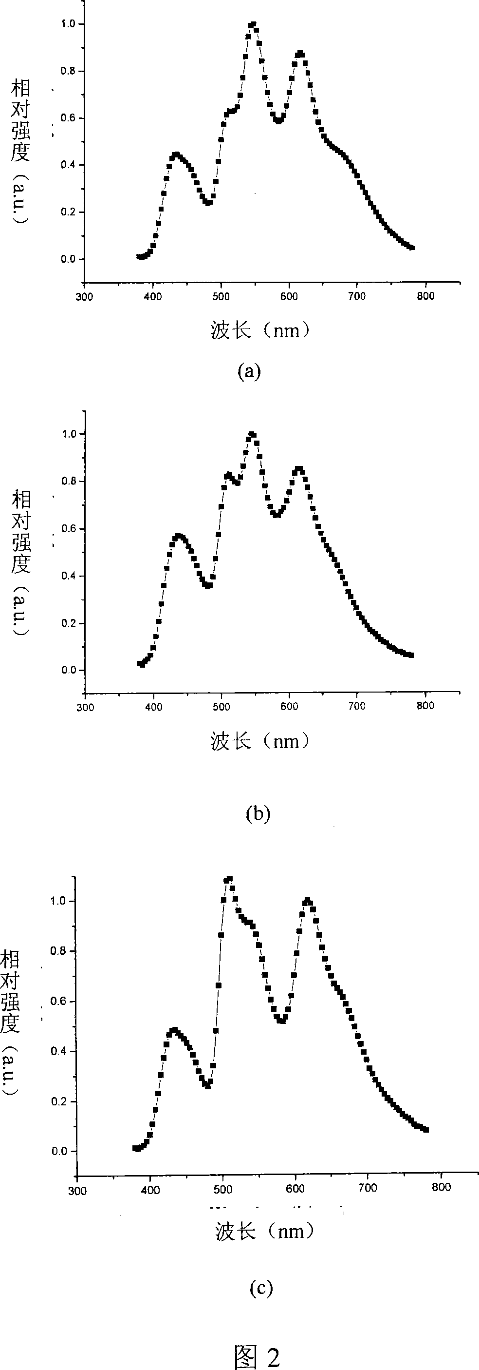
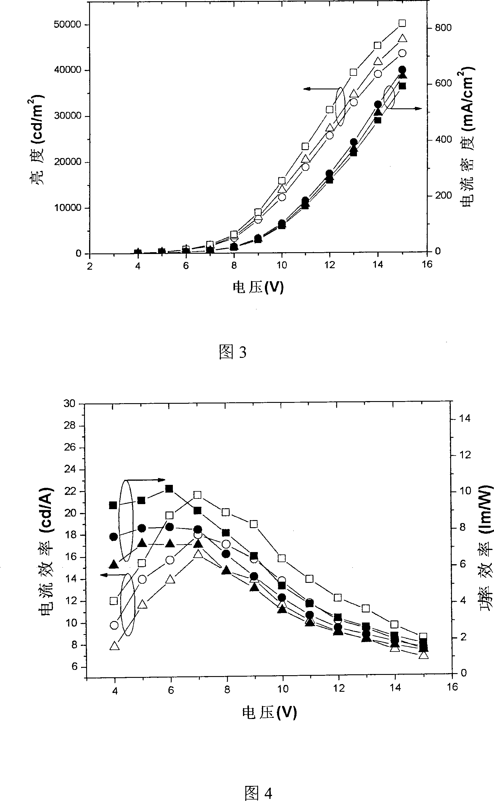
[0059] The electroluminescence spectrum of the device prepared in Examples 1-3 at a driving voltage of 7V is shown in Figure 2, the brightness-voltage, current density-voltage curves of the device are sho...


PUM


Abstract

This invention relates to an organic electro-white light device including a transparent chip, an anode layer, an organic cavity injection layer, an organic cavity transmission layer, an organic light emission layer, an organic cavity blocking layer, an electronic transmission layer and a cathode layer, in which, the organic light emission layer is a multi-layer structure composed of a blue emission layer, a green emission layer, a yellow and a red lamination layer, the blue layer emits fluorescent light and the other two emit phosphorescence, a matrix material of double transmission polarities is added between two phosphorescence layers to eliminate energy transfer between them and exchange positions of the two layers to increase the radiation effect and brightness of the devices.

Description

technical field [0001] The invention belongs to the field of organic electroluminescent devices, in particular to an organic electroluminescent device with multiple light-emitting layers. Background technique [0002] In recent years, with the in-depth study of organic materials, new organic materials have emerged continuously, and more understanding of its luminescent mechanism has been obtained. On this basis, the application research and device development of electroluminescence of organic materials have been carried out, and great success has been achieved, which has become one of the current research hotspots of lighting devices and display devices. The research and development history of organic material electroluminescent devices is not long, but it has shown strong vitality: it has active luminescence, low driving voltage (less than 10V), can display various colors, fast response speed, wide viewing angle, etc. advantages, and its lifespan is gradually approaching p...

Claims


Application Information

Patent Timeline
Patent Type & Authority Applications(China)
IPC IPC(8): H01L51/50H01L51/54H05B33/14
Inventor 李江段羽赵毅张利英刘式墉李斌李传南谢文法侯晶莹
Owner JILIN UNIV
Why Eureka
Try Eureka