

Organic light emitting device and method of preparing the same
a light-emitting device and organic technology, applied in the field of organic light-emitting devices and methods of preparing the same, can solve the problems of unsuitable mass production of conventional oleds, and achieve the effect of low cost and high yield of oleds
- Summary
- Abstract
- Description
- Claims
- Application Information
AI Technical Summary
Benefits of technology
Problems solved by technology
Method used
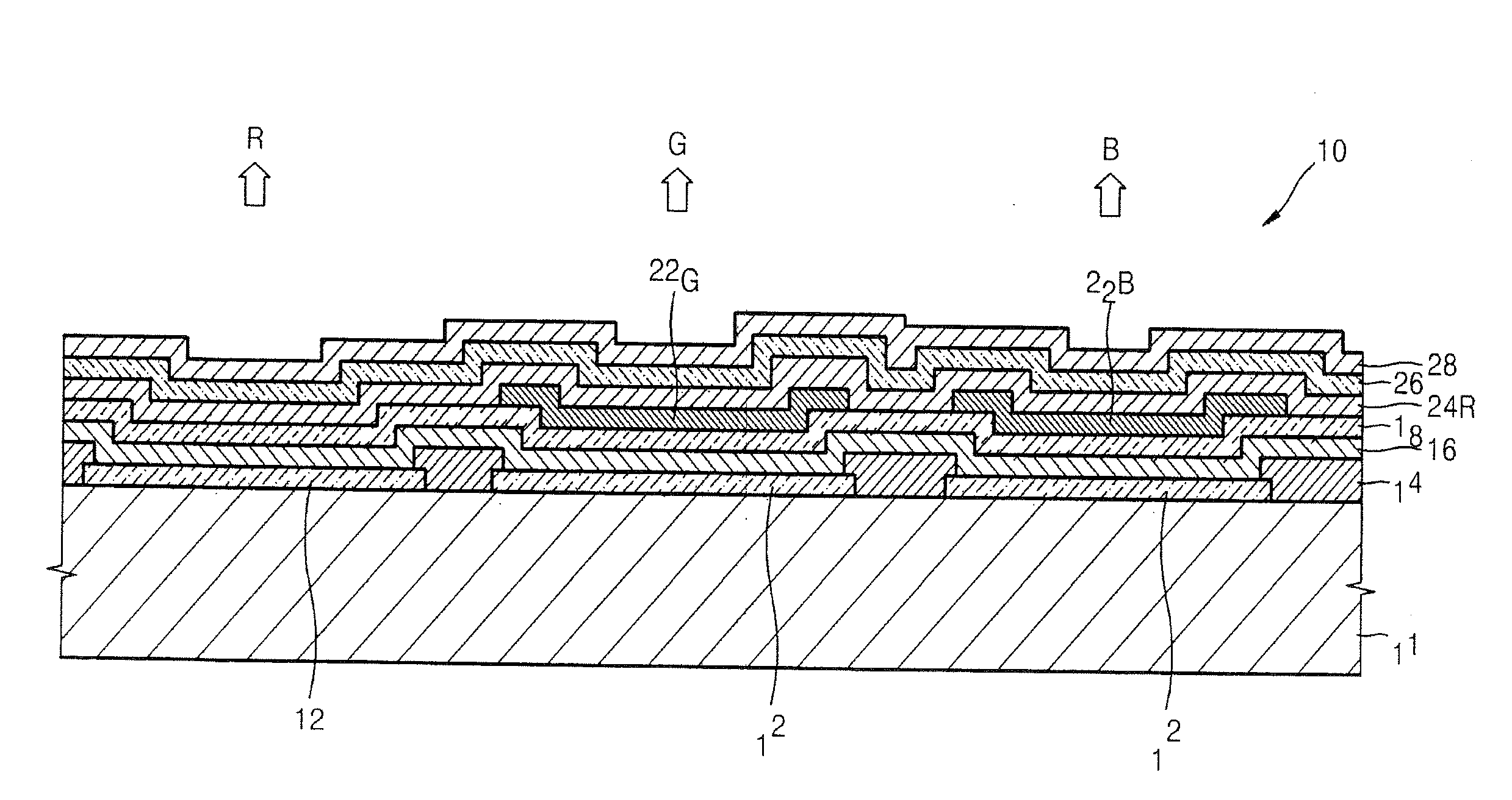
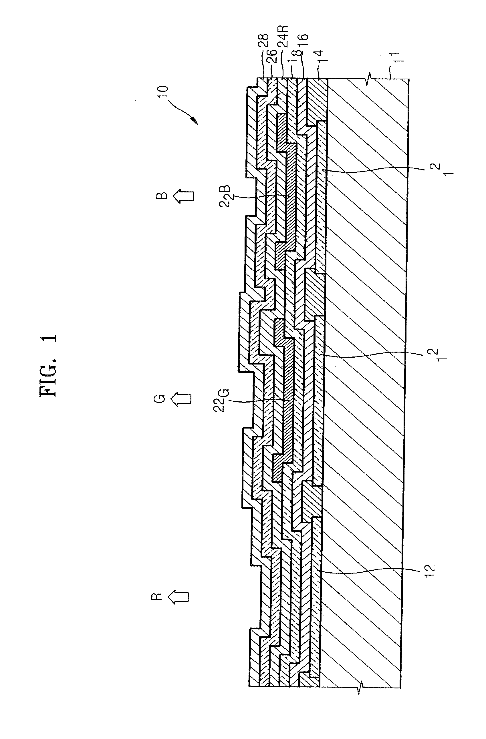
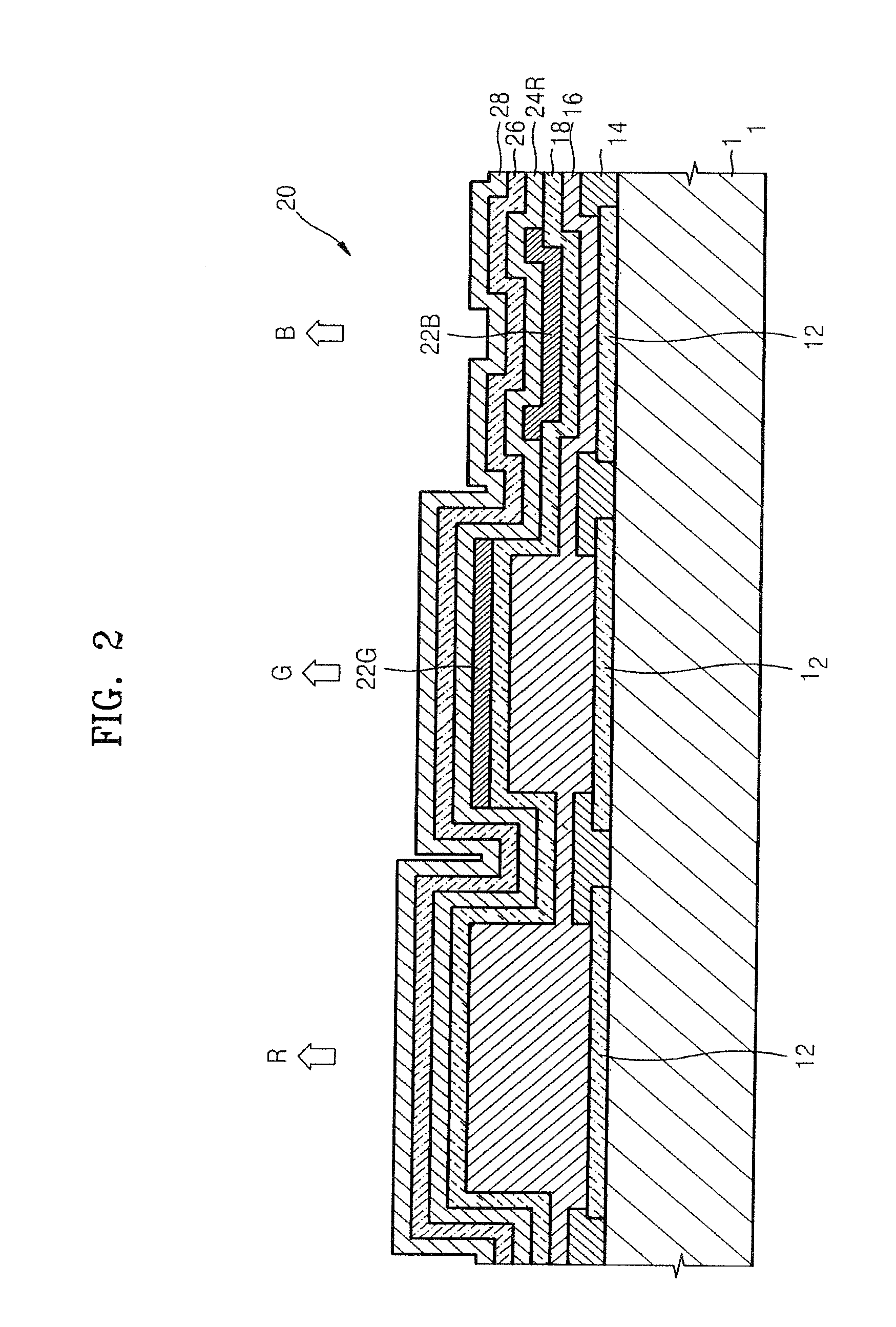
Image

Examples
example 1
Measurement Example 1
[0115]The efficiency and lifetime of the OLEDs prepared according to Example 1 and Comparative Example 1 were measured using a PR650 (Spectroscan) Source Measurement Unit and McScience Polaronix M6000. The results are shown in FIGS. 7 and 8.
[0116]Referring to FIG. 7, the OLED prepared according to Example 1 showed higher efficiency than the OLED prepared according to Comparative Example 1.
[0117]Referring to FIG. 8, the OLED prepared according to Example 1 showed a longer lifetime than the OLED prepared according to Comparative Example 1.
[0118]Electroluminescence (EL) spectrums of the OLEDs prepared according to Example 1 and Comparative Example 1 were measured using a Spectra Radiometer (PR650, Photo Researcher Inc.). The results are shown in FIG. 9. Referring to FIG. 9, the OLEDs prepared according to Example 1 and Comparative Example 1 showed maximum emission at about 520 nm, which indicates green emission.
Example 2
[0119]A 100 nm-thick Ag and ITO substrate (pr...
example 2
Measurement Example 2
[0124]The efficiency of the OLEDs prepared according to Example 2 and Comparative Example 2 were measured using a PR650 (Spectroscan) Source Measurement Unit and a McScience Polaronix M6000. The results are shown in FIG. 10.
[0125]The efficiency results for the OLED prepared according to Example 2, shown in FIG. 10, depict the errors which can occur from the resonance structure. It is expected that if the color coordinates of the two OLEDs are tuned, the efficiency of the OLED prepared according to Example 2 will be higher than that of the OLED prepared according to Comparative Example 2.
[0126]EL spectrums of the OLEDs prepared according to Example 2 and Comparative Example 2 were measured using a Spectra Radiometer (PR650, Photo Researcher Inc.). The results are shown in FIG. 11. Referring to FIG. 11, the OLEDs prepared according to Example 2 and Comparative Example 2 showed maximum emission at about 630 nm, which indicates red emission.
[0127]As described above,...
PUM
| Property | Measurement | Unit |
|---|---|---|
| temperature | aaaaa | aaaaa |
| thickness | aaaaa | aaaaa |
| thickness | aaaaa | aaaaa |
Abstract
Description
Claims
Application Information