

Oscillation circuit and method of controlling same
A technology of oscillating circuits and circuits, applied in power oscillators, electrical components, generating electric pulses, etc., can solve problems such as inability to form oscillating circuits, and achieve the effects of shortening start-up time and suppressing current consumption
- Summary
- Abstract
- Description
- Claims
- Application Information
AI Technical Summary
Problems solved by technology
Method used
Image

Examples
Embodiment 1
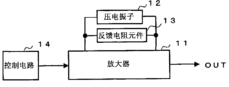
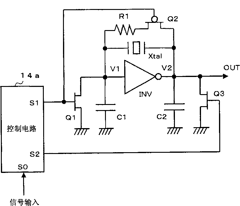
[0035] figure 2 It is a circuit diagram of an oscillation circuit according to the first embodiment of the present invention. exist figure 2 Among them, the oscillation circuit includes a CMOS structure inverter circuit INV, a crystal oscillator Xtal, a resistance element R1, capacitance elements C1 and C2, NMOS transistors Q1 and Q3, a PMOS transistor Q2, and a CMOS structure control circuit 14a.
[0036]The inverter circuit INV functions as an amplifier, and one end of the capacitive element C1, the drain of the NMOS transistor Q1, one end of the crystal oscillator Xtal, and one end of the resistive element R1 are connected to the input end. Furthermore, one end of the capacitive element C2, the drain of the NMOS transistor Q3, the other end of the crystal oscillator Xtal, and one end of the PMOS transistor Q2 are connected to the output end. The other end of the PMOS transistor Q2 is connected to the other end of the resistance element R1. The other end of the capaciti...
Embodiment 2
[0047] Figure 4 It is a circuit diagram of an oscillation circuit according to a second embodiment of the present invention. exist Figure 4 in, with figure 2 The same reference numerals denote the same components, and descriptions thereof are omitted. The oscillating circuit of the second embodiment with figure 2 In contrast, the NMOS transistor Q1 and the PMOS transistor Q2 are removed, and a 2-input NAND circuit NAND is provided instead of the inverter circuit INV. In addition, the control circuit 14b has a terminal S1B, and the output from the terminal S1B to one input terminal of the NAND circuit NAND and the slave figure 2 Inverted signal of the signal output by terminal S1. One end of the resistance element R1, one end of the capacitance element C1, and one end of the crystal oscillator Xtal are connected to the other input end of the NAND circuit NAND. Furthermore, one end of the capacitive element C2, the other end of the crystal oscillator Xtal, the other e...
Embodiment 3
[0056] Figure 6 It is a circuit diagram of an oscillation circuit according to a third embodiment of the present invention. exist Figure 6 in, with figure 2 The same reference numerals denote the same components, and descriptions thereof are omitted. The oscillating circuit of the 3rd embodiment with figure 1 In contrast, the NMOS transistor Q1 and the PMOS transistor Q2 are removed, and a 2-input NOR circuit NOR is provided instead of the inverter circuit INV. The terminal S1 is connected to one input end of the NOR circuit NOR. One end of the resistance element R1, one end of the capacitance element C1, and one end of the crystal oscillator Xtal are connected to the other input end of the NOR circuit NOR. Furthermore, one end of the capacitive element C2, the other end of the crystal oscillator Xtal, the other end of the resistive element R1, and the drain of the NMOS transistor Q3 are connected to the output end of the NOR circuit NOR.
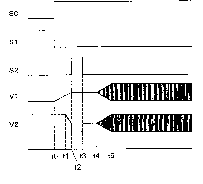
[0057] Next, the operation ...
PUM
 Abstract
Description
Claims
Application Information